|
|
Bachelor's Degree in Telecommunications Systems and in Network Engineering |
|
|
|
||
|
|
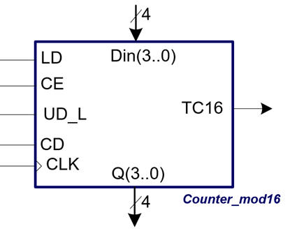
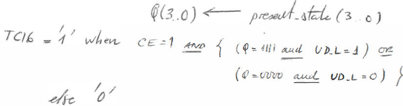
Counter_mod16: 4-bit radix-2 synchronous universal counter |
|
|
|
||
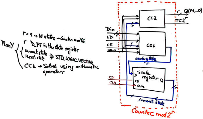
Plan Y: STD_LOGIC_VECTOR to define state signals and VHDL arithmetic library
| 1. Specifications | Planning | Developing | Test functional | Test gate-level | Report | Prototype |
Design the component Counter_mod16, that is a synchronous (CLK) reversible (UD_L) expandable (CE and TC16) 4-bit binary counter in radix-2 type 74ALS169 with parallel (LD, Din) inputs. This last feature allows the component to behave as a 4-bit data register as well. Use the plan Y based on the VHDL arithmetic library rec.
To better comprehend the circuit specifications, this is Counter_mod16.pdsprj implemented in Proteus using classic chips.
The sequence to follow to design a FSM in CSD. There is nothing in engineering like repeat and repeat again a procedure that works all the time for many applications. It is the company's know-how and means quality and reliability for manufactured products.
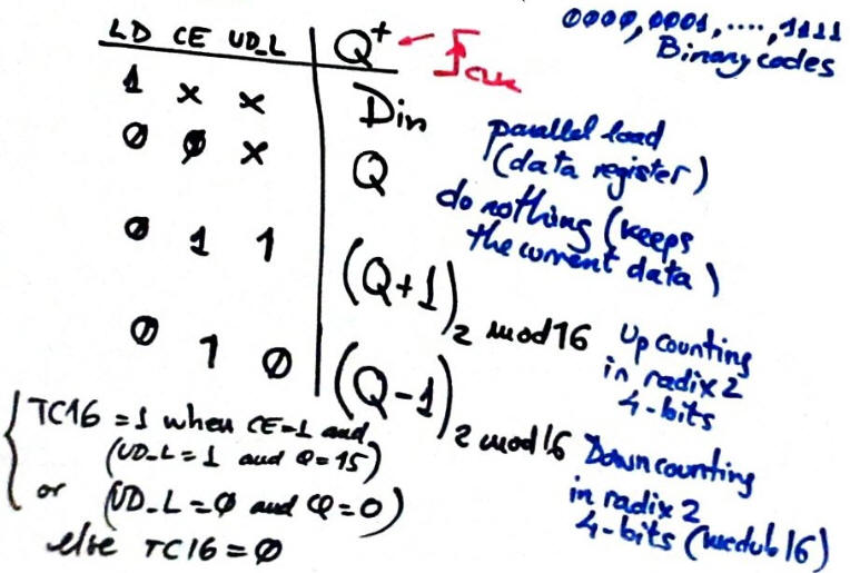
a) Draw the project symbol (Visio) and explain how the circuit works using a function table.
 |
|
|
| Fig. 1. Symbol (Visio) and function table of the Counter_mod16. |
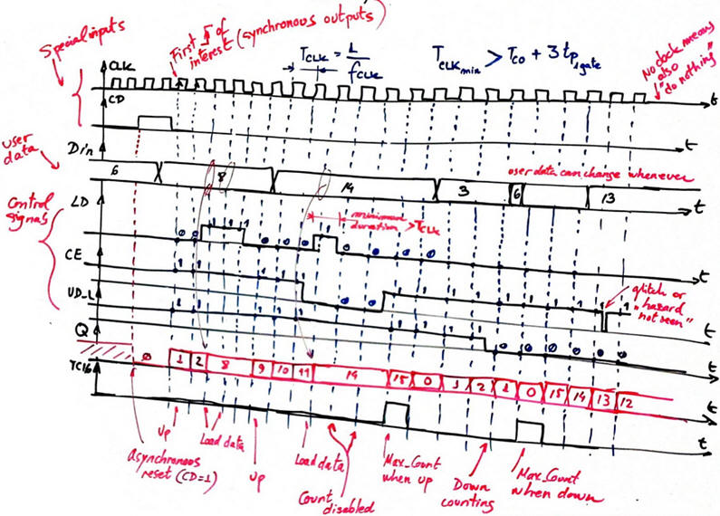
b) In this Chapter 2 representing the system evolving in time is a fundamental idea: draw a sketch of timing diagram. Fig .2 shows an example to visualise the four modes of operation.
 |
||
| Fig 2. Example of a timing diagram. | ||
| Specifications | 2. Planning | Developing | Test functional | Test gate-level | Report | Prototype |
Let's use the plan Y for inventing counters consisting of FSM using STD_LOGIC_VECTOR and arithmetic libraries.
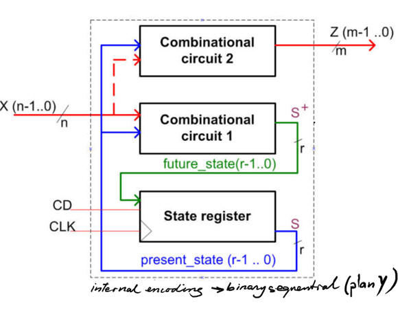
c) Draw the general architecture of FSM that you know can be applied to any synchronous sequential circuit, therefore, also here in this Counter_mod16. Is will become a single VHDL file with three processes (plan C1)
 |
|
| Fig 3. General architecture of FSM. | |
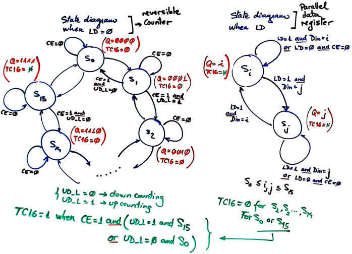
d) Draw the state diagram of Counter_mod16 and infer the number of registers required in this project when encoding states in binary sequential. In plan Y we use binary sequential (radix-2) in all designs.
 |
|
| Fig 4. State diagram. | |
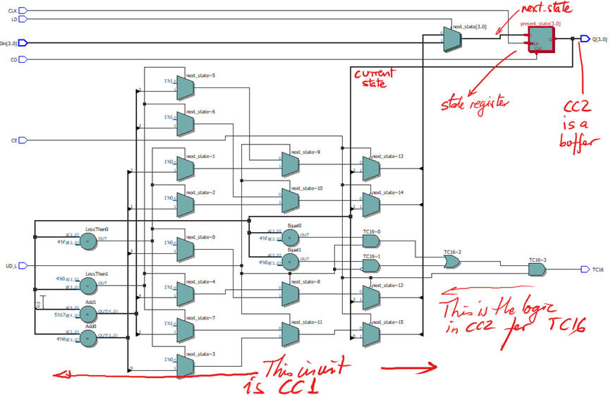
e) Adapt the general FSM topology to this problem as shown in Fig. 5. To which block (CC1, CC2, state register) is connected every input and output? The number of bits r required for coding current and next state signals is r = 4 for modulo 16.
 |
|
Fig 5. Adapting the FSM to this problem. This circuit can be easily expanded to the required counting capacity, for instance, with r = 24 it is possible to encode a very large counter of 16777216 states. And this is definitely a huge advantage over an alterative architecture based on plan C2. |
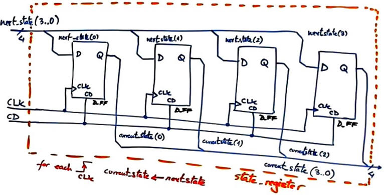
Draw the schematic of the state register (even if we know that it will be described all the time in the same way in VHDL as a process).
 |
|
| Fig 5. State register based on D_FF, the r = 4 memory cell to save the machine's current state. |
|
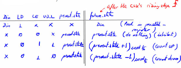
f) Write the truth table of CC2 and its equivalent behavioural (plan B) interpretation in flowchart. CC2 is for calculating outputs, thus, this combinational circuit takes care of all the signals drawn in parenthesis in the state diagram.
 |
|
Fig 6. CC2 truth table and flowchart. In this example, PROCESS is not required for translating CC2 equations to VHDL. Counter outputs Q(3..0) are simply a copy of the current_state and only buffers are synthesised. |
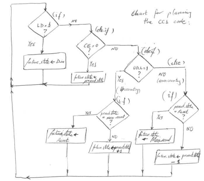
g) Write the truth table of CC1 and its equivalent behavioural (plan B) interpretation in flowchart. CC1 is for calculating the next state to go, thus, this combinational circuit takes care of all the circuit state transitions (arrows).
   |
|
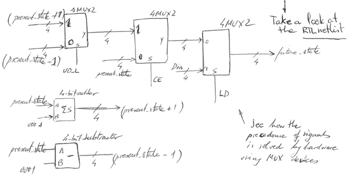
Fig 7. Truth table for CC1 circuit. Flowcharts for CC1 and also its interpretation using an structural circuit based on arithmetic and logic combinational circuits. Such circuits are correctly synthesised by EDA tools. |
Project location and file name:
C:/CSD/P7/Counter_mod16/(files)
| Specifications | Planning | 3. Developing | Test functional | Test gate-level | Report | Prototype |
h) Write the VHDL file (plan C1, a single file containing three processes representing the translation of the FSM. This is the complete Counter_mod16.vhd VHDL description.
i) Start a new project Counter_mod16_prj and run EDA synthesis tool for a CPLD or FPGA target chip. Let us choose Cyclone III 3C16F484C6N populating Terasic DE0 board.
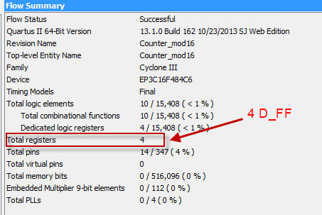 |
Fig 8. Project summary to observe resource utilisation like the number of registers and logic elements. |
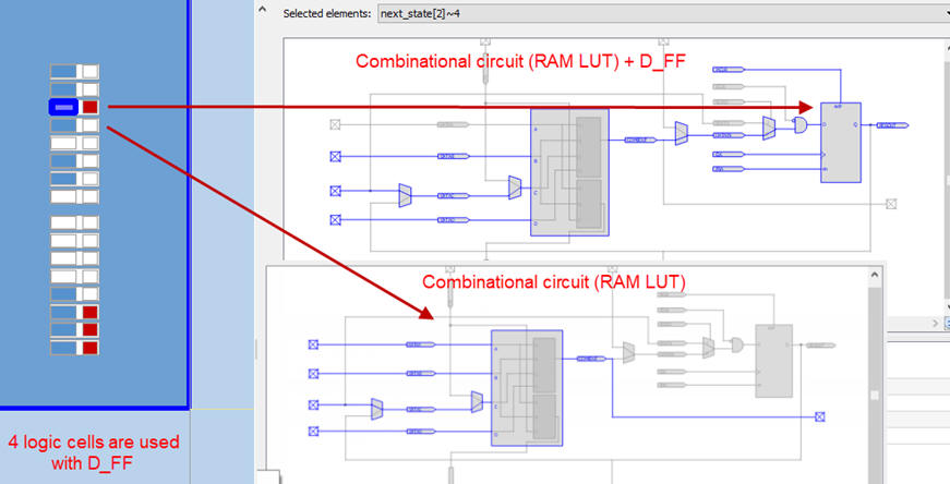
j) Discuss RTL and technology schematics. Check the number of registers (D_FF) used.
 |
| Fig 9. RTL view. |
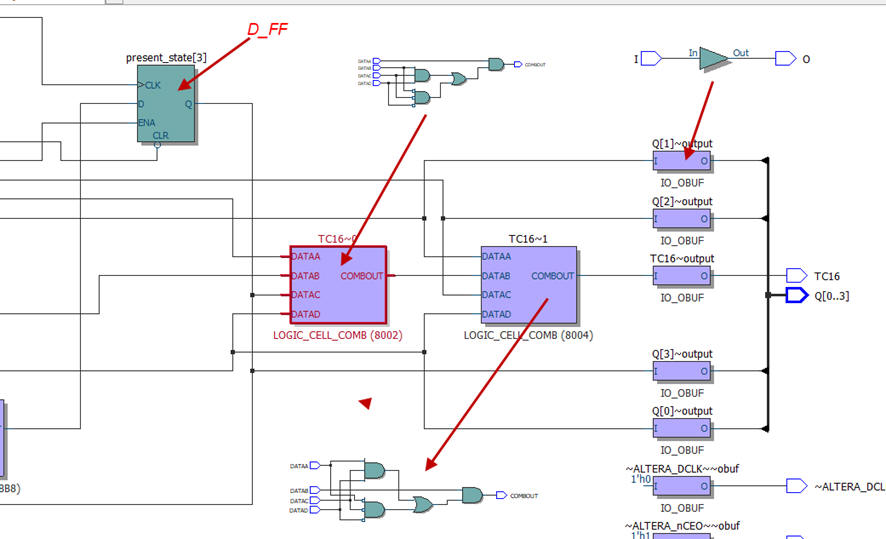
Is it possible using this plan Y inspect the state diagram as it was the case for plan X? Discuss the technology schematic. Can you identify similar blocs like the ones discussed in the planning section?
 |
|
|
Fig 10. Technology view. Can you compare and discuss this circuit with the schematic proposed for instance for the 74VLC169 classic chip? (full schematic). |
|
Another tool of interest is the Chip Planner. It allows visualising the silicon implementation zooming down at the floor-plan level to analyse critical paths and routings, logic elements and D_FF locations and many other details of the real circuit configured in the chip. It is an advanced feature out of the scope of our CSD introductory course. This is a definitive advantage of professional EDA tool: infer what is ahead of you if you engage an advanced course in hardware design.
 |
|
| Fig 11.Example of chip planner visualisation. | |
| Specifications | Planning | Developing | 4. Test functional | Test gate-level | Report | Prototype |
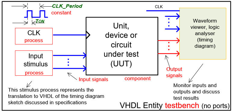
k) Draw a sketch of the testbench fixture.
 |
|
| Fig 12. Test bench fixture. | |
Start the test bench template and add the CLK and inputs activity translating the timing diagram. Make all the timing relative to the CLK_Period constant. Example file Counter_mod16_tb.vhd.
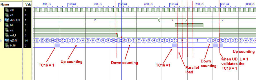
l) Run the EDA VHDL simulator tool and demonstrate how the circuit works adding comments to the printed sheet of paper containing the waveforms. Your system may works like the timing diagram discussed in class.
 |
||
| Fig 13. Example of a functional simulation of the universal counter modulo 16. The comments in red ink are very important to check whether the circuit works as expected. | ||
| Specifications | Planning | Developing | Test functional | 5. Test gate-level | Report | Prototype |
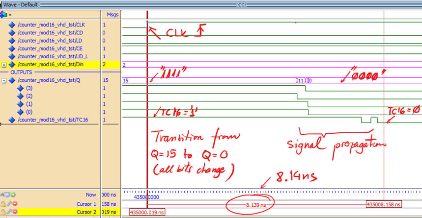
m) Run a gate level simulation and simulate the technology circuit (flat vho, sdo or sdf) using your VHDL test bench and discuss results. Measure the maximum speed of the counter deduced from the propagation time from CLK to output (tCO).
 |
|
 |
|
|
Fig 14. Example of a gate-level simulation in a CLK transition and measurement of propagation delay from CLK to output (tCO). |
|
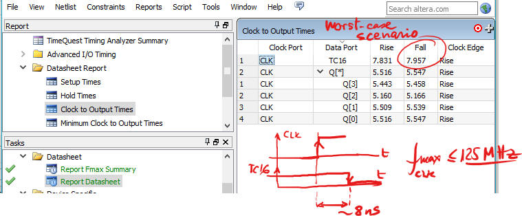
n) Run the timing analyser tool to deduce the maximum CLK frequency that can be applied to your design considering a target chip.
 |
|
|
Fig 15. Example of a timing analyser spreadsheet representing CLK to output delays (tCO) so that the worst-case scenario is the longest delay and thus the maximum frequency. |
|
Another interesting experiment to be carried out is to run a gate-level simulation setting the CLK_Period parameter near the minimum value. Discuss the results.
| Specifications | Planning | Developing | Test functional | Test gate-level | 6. Report | Prototype |
Follow this rubric for writing reports.
| Specifications | Planning | Developing | Test functional | Test gate-level | Report | 7. Prototype |
Use a laboratory training board and perform measurements to verify how the circuit works. For instance the DE10-Lite. Two options may be considered to drive the CLK signal:
1. Generate CLK pulses using an external push-button such KEY0, so that Counter_mod16 will determine the next state to go every time you click the button.
2. Implement our standard CLK_generator component as proposed in L8.2 to be able to generate for instance a 1.0 s time base (1 Hz) or any other frequency of interest from the quartz crystal oscillator, for instance 16Hz.
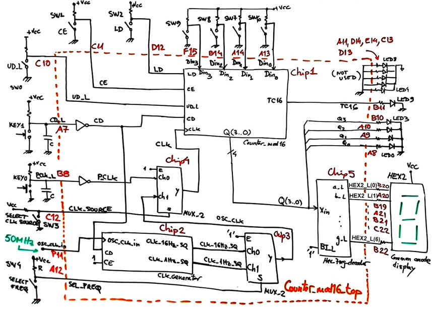
The schematic Counter_mod16_top for the prototype is drawn in Fig. 16. We include Chip5 for representing output hexadecimal symbols in a 7-segment display. Multiplexers allow us to choose a pair of oscillator CLK frequencies or generating CLK pulses manually clicking KEY0.
 |
|
|
Fig 16. Proposed schematic Counter_mod16_top for the prototype. |
|
This is the list of VHDL files included in this top design Counter_mod16_top.zip.
 |
|
|
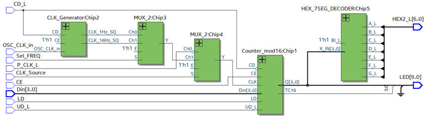
Fig. 17. Counter_mod16_top RTL schematic. 31 D_FF are used in this top design: 21 + 4 + 1 +1 + 4. |
|
This is the file Counter_mod16_top_prj_pins.csv containing the pin assignment. It can be imported directly to Quartus Prime project.
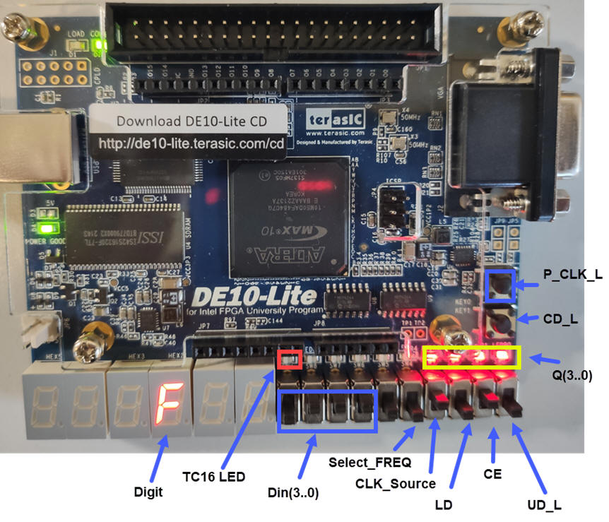
If you want to use only the programmer application, this is the final configuration file Counter_mod16_top_prj.sof for programming the FPGA MAX10.
 |
|
|
Fig. 18. Prototype running. |
|
- What is the problem when selecting CLK pulses from KEY0 push-button? How to solve it? Even if there is an analogue filter, we need a debouncing filter to generate clean digital pulses. How to improve this design adding such circuit?
| Home Term 26/27-Q1 Contact Products Electronic devices and companies Software Books Magazines Instruments DEE Library EETAC DEEL |

|
|
| Web activa des de 09/2001, @ F. J. Robert, Web editat amb Microsoft Expression Web 4. El contingut és un complement als materials d'estudi del curs Circuits i Sistemes Digitals disponibles al campus digital Atenea. Llicència:Reconeixement 4.0 Internacional de Creative Commons |