|
|
Bachelor's Degree in Telecommunications Systems and in Network Engineering |
|
(A) Synchronous data registers, (B) 1-bit data register |
Standard sequential components
| 1. Specifications | Planning | Developing | Testing (functional) | Testing (gate-level) | Prototype | Report |
The idea of this tutorial is to propose the design of a n-bit parallel register, a controllable memory cell for a n-bit word. Two strategies are possible: plan Y and plan C2, and thus we propose to compare them.
Let us start design a 4-bit data register as a FSM based on plan Y (state signals defined as STD_LOGIC_VECTOR).
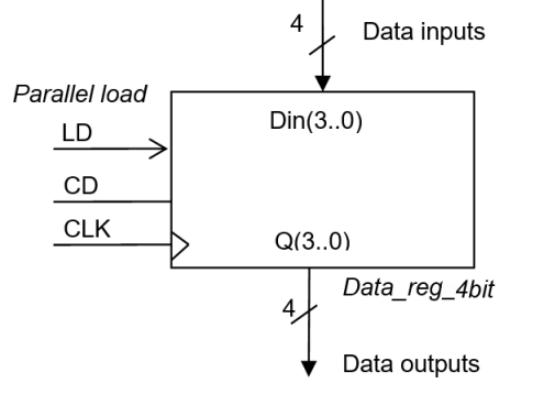 |
Fig 1. Symbol of the Data_reg_4bit block and function table describing how the circuit works. When LD (parallel load) signal is sampled high, Din is saved as the data output Q.
|
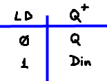
Draw an example of timing diagram as in Fig. 2 to show how the circuit works. Be aware how sample control input LD or and Din vector have to be stable before and after CLK active edges (setup and hold times).
|
|
|
Fig 2. Example of timing diagram showing when Din is sampled and when it is kept saved. |
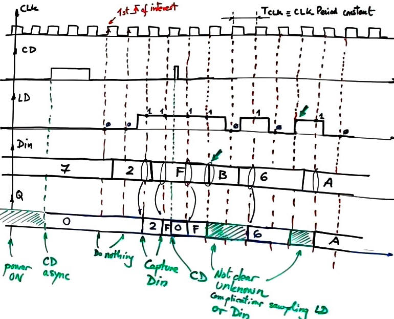
If we pay attention to the state diagram of such circuit as represented in Fig. 3, 16 values can be saved, thus it means a FSM up to 16 states. However, unlike counters, a large number of state transitions are possible (16 · 16 +16 = 272), from any state the register can jump to any other one. This architecture cannot be solved efficiently using plan X naming and labeling states and encoding them using any binary code as it was done in P6 applications or small counters such Counter_BCD_1digit.
|
|
|
Fig 3. State diagram. |
| Specifications | 2. Planning | Developing | Testing (functional) | Testing (gate-level) | Prototype | Report |
Adapt the general FSM architecture to this project.
|
|
|
Fig 3. FSM adaptation to the state register. |
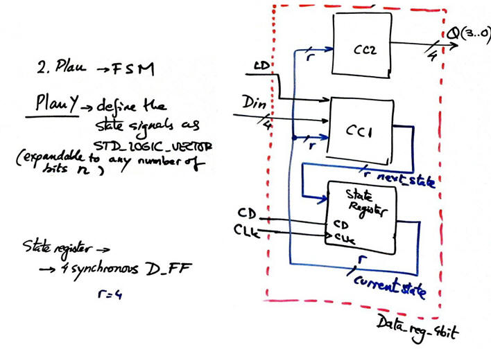
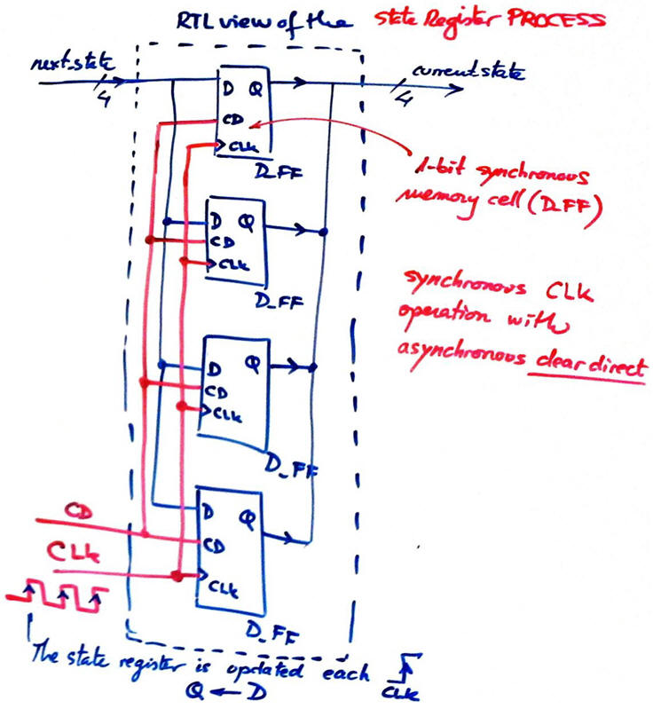
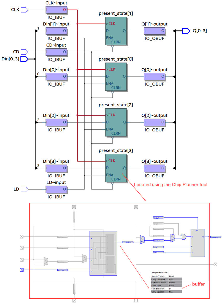
In Fig. 4 we see the structure of the FSM's state register. How many D_FF are used?
|
 |
|
Fig 4. State register consist of four D_FF working synchronously in parallel. |
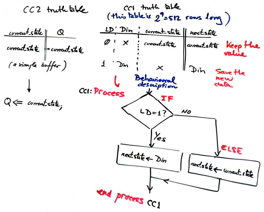
We can represent as well CC2 and CC2 truth tables and their equivalent as plan B flowcharts. Solving 272 states transitions is possible and simple to implement using STD_LOGIC_VECTOR signals as proposed in plan Y. Encoding FSM is solved in binary radix-2.
|
|
|
Fig 5. CC1 and CC2 truth tables and flowcharts. |
Project location:
C:\CSD\P7\Data_reg_4bit\(files)
Discussion on larger data registers, circuit expansion.
- How to invent Data_reg_nbit using plan Y? In the same way than the 4-bit data register, use n-size STD_LOGIC_VECTOR
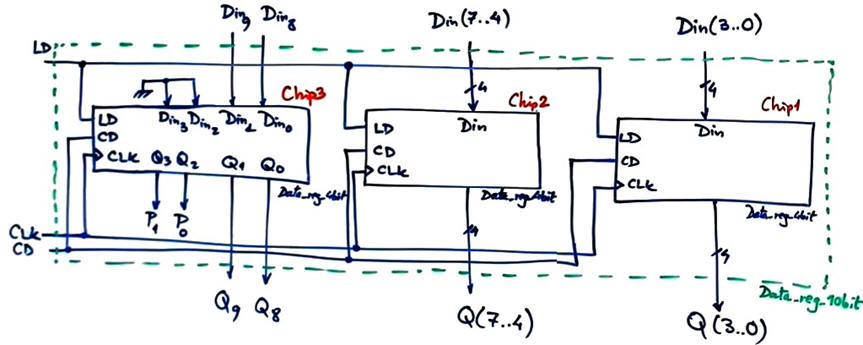
- How to invent Data_reg_nbit using plan C2? Data_reg_4bit can be wired in parallel to reach any data size n. For instance a Data_reg_10bit is represented in Fig. 6.
|
|
|
Fig 6. Data_reg_10bit using plan C2 and components Data_reg_4bit. |
- How to invent Data_reg_nbit using plan C2?
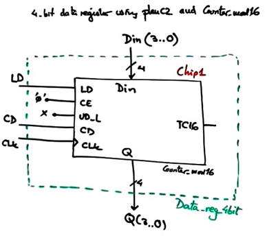
As shown in Fig. 7, universal counters such as Counter_mod16 forced to work always with CE = '0' or shift registers such as Shift_reg_4bit forced to work with S(1) = S(0) = LD, can also be used as parallel data register.
|
|
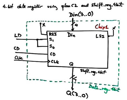 |
Fig 7. Two alternative ways to implement a 4-bit data register using standard components. |
|
| Specifications | Planning | 3. Developing | Testing (functional) | Testing (gate-level) | Prototype | Report |
Translate the plan schematic in a single VHDL named Data_reg_4bit.vhd.
Start a synthesis project for a given CPLD or FPGA target chip.
|
|
|
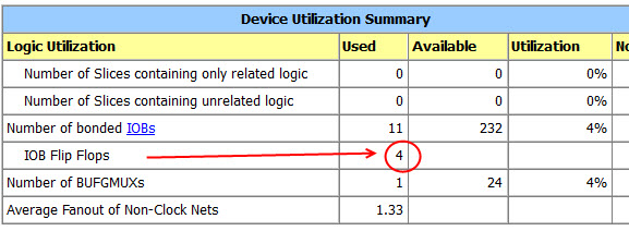
Fig 8. The summary spreadsheet has to show the four D_FF used. |
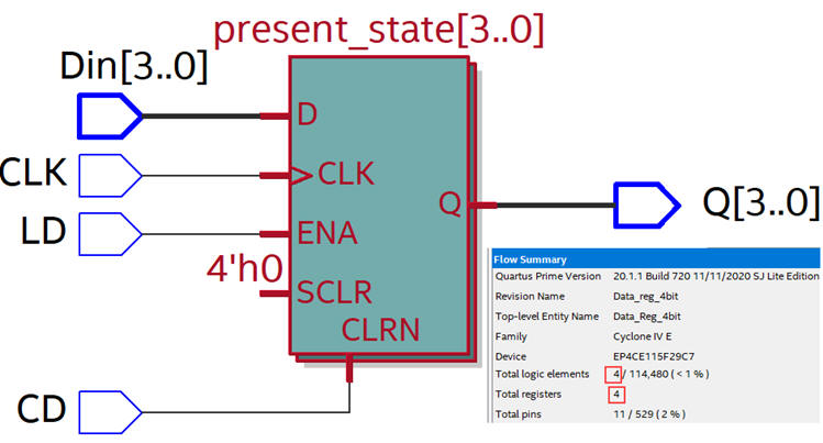
Print and discuss the RTL schematic.
|
|
|
Fig 9. RTL view. |
Print and comment the technology view. Fig. 10 shows the implementation in a Cyclone IV logic element. The D_FF already has an ENA (enable) additional input thus the LUT is simply used as a buffer for wiring input D.
|
|
|
Fig 10. Technology view. |
| Specifications | Planning | Developing | 4. Testing (functional) | Testing (gate-level) | Prototype | Report |
Draw the testbench fixture for testing the unit under test Data_reg_4bit and obtain its skeleton from Quartus Prime.
|
|
|
Fig 11. Testbench fixture for running VHDL simulations. |
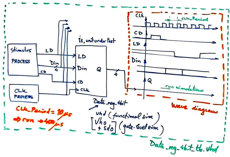
Translate the initial timing diagram sketch represented in Fig. 2 into a VHDL stimulus process for your testbench. Include as well constant CLK_Period. This example file can be used for copying constants and signal stimulus Data_reg_4bit_tb.vhd.
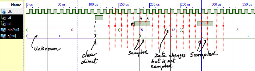
Run a ModelSim functional simulation and discuss results such in Fig. 12.
|
|
|
Fig 12. Example of a timing diagram. |
| Specifications | Planning | Developing | Testing (functional) | 5. Testing (gate level) | Report | Prototype |
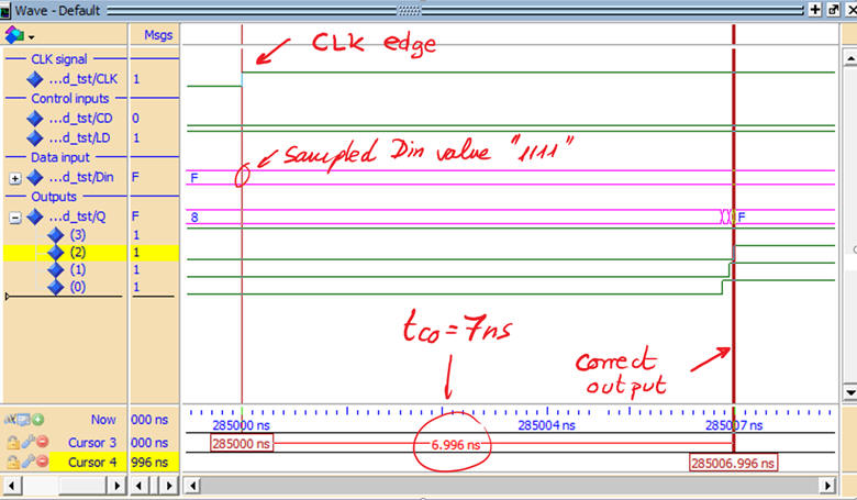
Start a gate-level ModelSim functional simulation and measure propagation time from CLK to output tCO.
|
|
|
Fig 13. Measuring tCO at a given active CLK edge transition. |
Compare results with timer analyser tool.
|
|
|
Fig 14. Timing analyser spreadsheet calculating worst-case tCO = 7 ns |
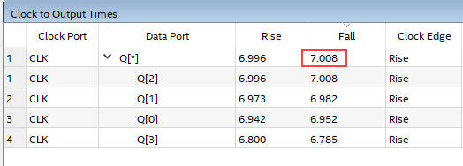
How many times per second a 4-bit digital input can be sampled? fMAX < 1/tCO = 142.8 MHz
Can this Data_reg_4bit be used for sampling HI-FI audio signals at 44.1 kHz compact disk standard?
And what about video signals?
And as a front-end sampling circuit in a logic analyser instrument working at 100 MHz sampling ratio?
| Specifications | Planning | Developing | Testing (functional) | Testing (gate-level) | 6. Prototype | Report |
Download the final configuration file to the PLD target chip populating the training board and perform laboratory measurements to verify how the circuit works.
An interesting circuit here in this experimentation area may a 4-bit digital acquisition system capable of sampling and reproducing at several CLK frequencies.
| Specifications | Planning | Developing | Testing (functional) | Testing (gate-level) | Prototype | 7. Report |
Follow this rubric for writing reports.
(A) Synchronous data registers, (B) 1-bit data register |
| 1. Specifications and plan | Developing | Testing | Prototype | Report |
The component 1-bit data register is very useful to save 1-bit data such as status signals from datapaths, or simple digital sensors sampled under control of a FSM. As represented in Fig. 1, it is exactly as the circuit above reducing the data size to n = 1bit. Therefore, there is no need to follow a full project design because we can derive immediately its plan Y in a single file or use plan C2 considering any of the 4-bit from the component above.
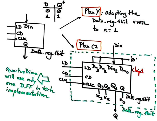 |
| Fig. 1. Symbol and two plans for the Data_reg_1bit. |
| Specifications and plan | 3. Developing | Testing | Prototype | Report |
For either plan, only one D_FF is used.
Plan Y: Data_reg_1bit.vhd
Plan C2: Data_reg_1bit.vhd
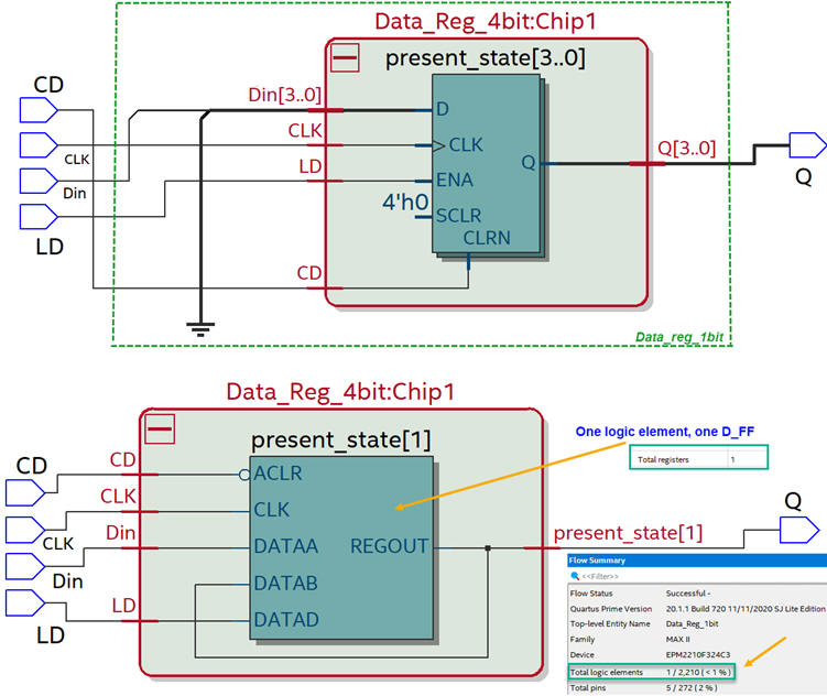 |
| Fig. 2. RTL and technology schematics. |
| Specifications and plan | Developing | 4. Testing | Prototype | Report |
Data_reg_1bit_tb.vhd
| Specifications and plan | Developing | Testing | 6. Prototype | Report |
| Specifications and plan | Developing | Testing | Prototype | 7. Report |
| Home Term 26/27-Q1 Contact Products Electronic devices and companies Software Books Magazines Instruments DEE Library EETAC DEEL |

|
|
| Web activa des de 09/2001, @ F. J. Robert, Web editat amb Microsoft Expression Web 4. El contingut és un complement als materials d'estudi del curs Circuits i Sistemes Digitals disponibles al campus digital Atenea. Llicència:Reconeixement 4.0 Internacional de Creative Commons |