|
|
Bachelor's Degree in Telecommunications Systems and in Network Engineering |
|
Chapter 2 problems |
- D2.3 - |
LED rotator (FPGA-VHDL) |
1. Specifications
Our aim is to implement in a target FPGA a LED rotator like the one represented in Fig. 1, which is basically a FSM acting as an 8-bit one-hot shift register that runs continuously. The same project designed programming a μC is in D3.3.
The system operates by means of clicking several times the same push-button, sampled at 250 Hz, as other similar commercial products like the Light control in LAB6 and the Flashing_lamp example for a bike torch. After turning on the circuit's power supply switch, the LED array is initially off.
- First click: all LED on.
- Second click: shift and rotate right at 2.5 Hz
- Third click: shift and rotate left at 5 Hz
- Fourth click: light intensity modulation and toggle flashing at 7.5 Hz four LED at a time: even LED at full intensity; odd LED at half light intensity.
 |
|
Fig. 1. LED_rotator symbol and idea. |
2. Planning
Design phase #1: basic features. FSM architecture and current state encoding, asynchronous reset (CD), system clock (CLK), sampling input values, synchronous systems, maximum speed of operation, etc. Solve the circuit for the design step #1. This means covering P5 and P6 circuits, concepts and ideas.
At this initial stage, we can imagine the application blocks, which forcibly has to be engineered in several steps and phases. Features such a real-time clock and the CLK_Generator are added in the in the second design phase.
Light intensity can be modulated applying less power to the LED. For instance, driving a LED with a '1' means maximum power and light intensity. In this way, if we apply 1 kHz squared signal, it will be integrated by the eye so that the user will see half light intensity. Adjusting pulse duration (PWM) allows light intensity modulation.
   |
Fig. 2. Diagram and indications for some suggested blocks of the application for the design phase #1 to be used in steps #1 and #2. Be aware that another circuit will be required to select the rotator CLK frequency between 5 Hz and 2.5 Hz. |
Project location:
C:\CSD\P6\LED_rotator\(files)
- Design step #1. Consider an initial circuit to generate several binary codes to detect the sequence of PB clicks.
Fig. 2 shows the basic FSM that will have the functionality of detecting PB clicks. In this way, the final LED signals and clock frequencies can be designed in next steps.
Draw the FSM Chip1 state diagram. Fig. 4 shows an example where up to ten states can be identified to memorise the number of push-button clicks by means of a binary radix-2 code at output vector CNTL.
 |
|
Fig. 3. State diagram example. Complete and discuss it. |
Sketch a timing diagram showing the main operations and also imagining state values. These stimulus signals can be applied in section fourth in the testbench process translated to VHDL.
 |
|
Fig. 4. Timing diagram example. |
Adapt the FSM architecture to this problem, naming and connecting all signals and inputs and outputs. This will be translated as a single plan C1 VHDL file. Deduce how many D_FF are required when encoding FSM states using the following options and draw the state register memory:
Option #1: Radix-2 (sequential)
Option #2: Gray
Option #3: Johnson
Option #4: One-hot
|
|
|
Fig. 5. FSM adaptation to the problem. |
Write the CC2 truth table to obtain the outputs of the circuit and its flowchart.
|
|
|
Fig. 6. CC2 truth table and its equivalent plan B flowchart ready for VHDL translation. |
Design the CC1 truth table to obtain the next state to go and its flowchart.
|
|
|
Fig. 7. CC1 truth table and its equivalent plan B flowchart ready for VHDL translation. |
3. Development
Write the VHDL file.
Start a Quartus Prime synthesis project for one of the following programmable target chips:
Option #1: Cyclone IV EP4CE115F29C7
Option #2: MAX II EPM2210F324C3
Option #3: MAX 10 10M50DAF484C7 (for gate-level simulations, choose one of the previous options)
Inspect and discuss the RTL and technology schematics. Check the number of D_FF.
|
|
|
Fig. 8. RTL schematic generated by Quartus Prime and project summary where we can check the resources used and the number of D_FF. |
|
|
|
Fig. 9. Technology view where we can indicate and count the number of D_FF of the state register. |
4. Testing functional
Draw the testbench fixture, add stimulus processes to the VHDL template and run the EDA simulation tool to verify your design. Discuss your results on the wave pictures.
|
|
|
Fig. 10. Testbench fixture schematic for the basic FSM in step #1. |
|
|
|
Fig. 11. Waveforms showing the full cycle of signals and internal states of the automata. |
5. Testing (gate-level)
Measure the maximum CLK frequency related to tCO that can be applied to your design considering your target chip.
|
|
|
Fig.12. Example of gate-level simulation to measure the propagation time from CLK to output (tCO). |
- Design step #2. Add the datapath and its components to the basic structure from atep #1, as advancing to cover P7 circuits, so that you can generate the specified LED sequences.
Go ahead with the step #2 only when step #1 is fully tested working correctly and its report is written. Explain how the new symbol will look like, use a dotted box as usual in CSD, what are the modifications for the new features, new inputs (f it is the case), and outputs. What components will contain the datapath. Etc.
Project location:
C:\CSD\P7\LED_rotator\(files)
Design the Rotator_8bit in Fig. 2 using one of these architecture options:
Option #1: Plan C2 designing firstly a Shift_reg_8bit component using standard Shift_reg_4bit.
Option #2: Plan Y in a single file.
Design phase #2: dedicated processor, real-time, advanced features.
Only when design phase #1 in its two steps is fully tested working correctly and reported, solve the design phase #2 as advancing to cover P8 materials.
Project location:
C:\CSD\P8\LED_rotator\(files)
- Design step #1: Design a CLK generator to obtain all the necessary CLK signals from the target board quartz crystal oscillator (50 MHz). Deduce the number of D_FF required for this subcircuit.
- Design step #2. Design a count-down real-time clock and an electronic switch so that after being 2 minutes in OFF state the battery is disconnected to save energy. In this way we will replace the passive mechanical power switch by another power-on button and an electronic circuit. This feature related to energy saving, is implemented in Chapter 3 using a microcontrollers in its sleep mode.
- Design step #3. Imagine a sensor vector input generating codes like in the Tank_level_meter example to simulate monitoring the battery voltage. When this level is 80% a red LED goes flashing at 1 Hz to signal this low-battery condition, so that the used can recharge the application.
Hint: Suggested report organisation (similarly for slides presentation)
1. Specifications. First you explain all the specifications you like for your product. Add theory about anything of interest if necessary to comprehend the application.
2. Plan. Here you say that you have in mind several design phases and steps, each time incorporating only a few new features. And thus, that you simply will start developing and testing only what you have planned to be the first step.
3. Develop only the first step of the design phase #1
4. Test only the first step of the design phase #1
Annexes.
- Phase #1, step #2 (Datapath) Explain and do only what is modified in each of the previous sections to introduce the new features.
- Phase #2, step #1 (CLK_Generator) Explain and do only what is modified in each of the previous sections to introduce the new features. etc.
Chapter 2 problems |
- D2.3 - |
7-segment digit sequencer (FPGA-VHDL) |
1. Specifications
We want to design a driver to show a sequence of movement, clockwise and counter-clockwise, in a single 7-segment display. Fig. 1 represents the schematic diagram of the application. CLK signal to move segments is a 5 Hz rectangular wave. There is a switch to configure movement direction: CW = '1', clockwise; CW = '0' counter-clockwise.
The same project designed programming a μC is in D3.6.
 a) a)  |
|
Fig. 1. a) Circuit schematic. b) Digit segments and position when idle. c) Sequence of switching LED segments for CW = '1' clockwise or up-counting. |
Fig. 1c shows the sequence of segment lighting when CW = '1'. When the system remains idle, the only segment lighting continuously is g.
When clicking the push-button start/stop ST_L the system runs continuously in the configured direction.
When running, if ST_L is clicked again, the system stops after completing the sequence.
2. Planning
Better organise the design of a commercial product planning several phases.
Design phase #1: basic features.
Solve the circuit for the design step #1. Only when it is fully tested working correctly and reported, solve the design step #2.
Design step #1. Consider an initial circuit with no CW input, thus representing only clockwise movement.
Design step #2. Add the CW switch.
Let us start with the design step #1. Because of the requirement that the sequence must end only when completed after detecting an ST_L falling edge, we need a 1-bit memory cell to save this event when occurs, for instance an RS_Latch. When running, the FSM will generate the sequence as if it were counting in one-hot, one LED segment at a time. Therefore, this is a plan C2 system composed of a top design (sequencer) and some components.
Some questions to kick off the project.
Infer a circuit for solving this project. Fig 2 shows an initial example of internal design using two components. Once used (acknowledged), the ST_Flag has to be reset, thus, the FSM has to generate as well the internal signal CLR_F for the RS_Latch.
 |
|
Fig. 2. First idea of the Sequencer circuit internal architecture. CW switch is only to be considered for the design step #2. |
Firstly we will design the FSM chip, secondly we can proceed with the other components.
FSM
Imagine how the FSM circuit will work. Infer how many resources the circuit may contain and try to draw a state diagram for the circuit's FSM as shown in Fig. 3.
 |
|
Fig. 3. Idea of state diagram for this application. |
To see whether this proposed circuit and state diagram may work correctly, we can draw some waveforms in a timing diagram as in Fig. 4.
 |
| Fig. 4. Example timing diagram when clicking ST one time. Analysing the waveforms for a short click we see that the circuit presents complications because RS_latch inputs R = S = '1' for a while, generating an undefined signal that cannot be used as input by the FSM. |
Therefore, it is not clear that the circuit works as stated. How can we solve these complications driving correctly the RS_Latch? Can you solve the problem modifying the state diagram or the circuit?
The duration of the click depends on the user. We can have short clicks (TCLICK < 2 TCLK) and also long clicks (TCLICK > 2 TCLK). For example, the next analysis in Fig. 5 shows how a short click works correctly replacing the RS_latch by an RS_FF. However, a long user click invalidates the ST_Flag signal because R = S = '1' is still possible.
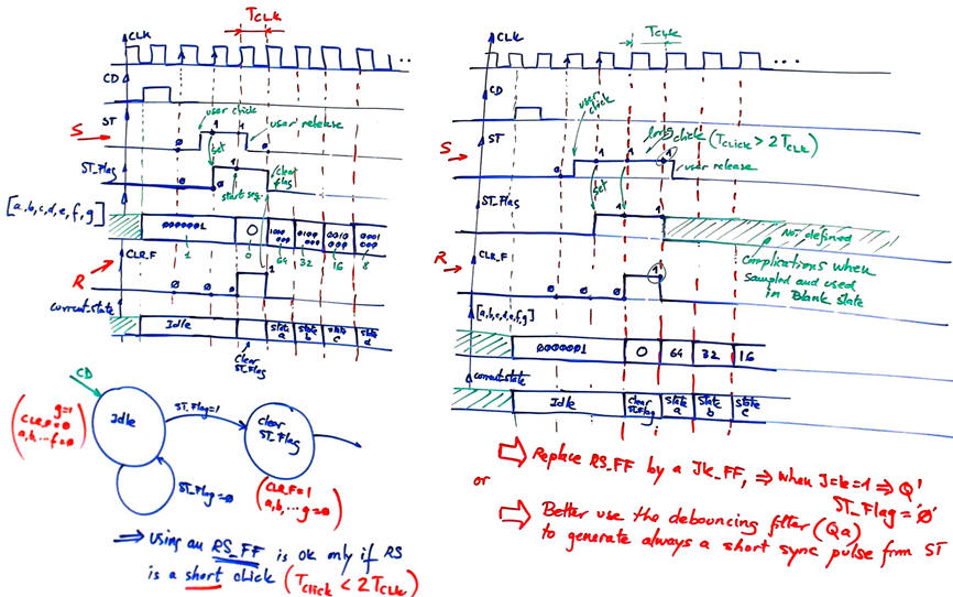 |
| Fig. 4. Analysis of a short and long click. |
Therefore, we can use a JK_FF as the Chip2 in Fig. 2. And we can continue the project in two ways:
(1) Imagining that the user generates always short pulses.
(2) Later, in new design steps, we can introduce extra hardware as Chip3 such the debouncing circuit to generate a single synchronous pulse when clicking (output Qa). In this way, ST will be always a short pulse.
Apply the FSM architecture to this problem.
Deduce how many D_FF are required when encoding FSM states using the following options and draw the state register memory:
Option #1: radix-2 (sequential)
Option #2: Gray
Option #3: Johnson
Option #4: one-hot
Draw the state register based on D_FF considering your state encoding option.
Write the truth table of CC2 and CC1 and their equivalent behavioural interpretations (plan B) using flowcharts.
Project location:
C:\CSD\P6\sequencer\(files)
Write the FSM VHDL file.
Start a Quartus Prime synthesis project for one of the following programmable target chips:
Option #1: Cyclone IV EP4CE115F29C7
Option #2: MAX II EPM2210F324C3
Inspect and annotate the RTL and technology views. Check the number of D_FF synthesised in this application.
Sequencer
Design the RS_Latch component using gates as in L5.1 or using SD and CD in a JK_FF or T_FF disabling the synchronous inputs with CLK = J = K = '0'.
Prepare a VHDL testbench fixture to adapt the stimulus signals in the Fig. 5 sketch. Rely on the constant CLK_Period for setting the time scale.
 |
|
Fig. 5. Testbench fixture. What inputs, outputs and internal signals are to be monitored? |
Run functional simulations to verify your design. Visualise as well in the wave timing diagram the internal states.
Measure the propagation time CLK to output (tCO)using gate-level simulations.
What may be a good estimation of the maximum frequency of operation? Explain your answer.
Design phase #2: Additional features to enhance the product such crystal oscillator for CLK signals nd timers for saving energy when the product is not used.
- Design step #1: Design a CLK generator to obtain the 5 Hz square wave from a 50 MHz quartz crystal oscillator like the one available in the DE10-Lite board. Deduce the number of D_FF that the Sequencer will contain.
- Design step #2: Add a Timer block so that after 2 minutes in Idle state, the system goes to a new Blank_sleep state to save energy, a kind of sleep mode. Clicking ST_L resumes operations.
- Design step #3: Modify the circuit adding a new input button PP (Play/Pause) that when clicked toggles the display. When in play mode, segments work as usual. When in pause, segments a-b-c-d-e -f blinks intermittently at 8 Hz.
Chapter 2 problems |
- D2.3 - |
5-bit Johnson counter (VHDL - FPGA) |
1. Specifications
Replicating the functionality of obsolete chips when they are required for some applications is always possible targeting programmable devices like FPGA or CPLD. Let us infer the classic chip 74HC4017 represented in Fig. 1, a Johnson decade counter, using VHDL and EDA tools from Intel such Quartus Prime and ModelSim Intel edition. target chip may be a Cyclone IV FPGA.
The same project designed programming a μC is in D3.20.
 |
Fig. 1. Internal structure of the chip implemented by NXP. |
Let us add and define the new features stated in Fig. 2.
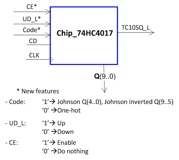 |
Fig. 2. Symbol adapted to our naming conventions and description of the chip functionality (Visio). |
Even if the schematic in Fig. 1 is is indicating an internal architecture based on several internal blocks (plan C2), you can use also plan A and plan B to solve this problem and compare circuit realisations and their respective performance.
Determine the maximum execution speed for the given target chip.
To make it easy, you can approach the problem in successive steps. For instance:
- Step 1: plan, design and test completely a 10-bit one-hot up counter with counter enable (CE) control signal.
- Step 2: copy your previous project source files in a new folder and add the feature up/down (UD_L) to make the device reversible.
- Step 3: copy your previous project source files in a new folder and add the output combinational function to translate Johnson to one-hot code (control signal Code).
| Home Term 26/27-Q1 Contact Products Electronic devices and companies Software Books Magazines Instruments DEE Library EETAC DEEL |

|
|
| Web activa des de 09/2001, @ F. J. Robert, Web editat amb Microsoft Expression Web 4. El contingut és un complement als materials d'estudi del curs Circuits i Sistemes Digitals disponibles al campus digital Atenea. Llicència:Reconeixement 4.0 Internacional de Creative Commons |