|
|
Bachelor's Degree in Telecommunications Systems and in Network Engineering |
|
Chapter 3 problems |
- D3.3 - |
Designing a LED rotator (µC - C) |
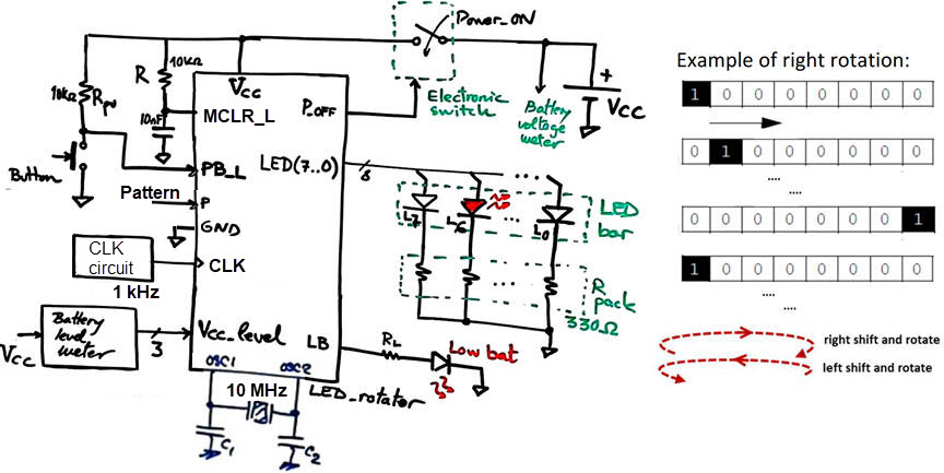
1. Specifications
Our aim is to implement the LED rotator in Fig. 1 as an application of FSM adaptation to µC as represented in Fig. 1. Our target microcontroller is the PIC18F4520.
The same project designed using hardware is stated in D2.3.
The system operates by means of clicking several times the same push-button; an external interrupt is generated by such event. After turning on the circuit's power supply switch, the LED array is initially off.
- First click: all LED on.
- Second click: shift and rotate right at 2.5 Hz
- Third click: shift and rotate left at 5 Hz
- Fourth click: light intensity modulation and toggle flashing at 7.5 Hz four LED at a time: even LED at full intensity; odd LED at half light intensity.
- P is a switch to select between two rotation patterns. When '0' the pattern is a code one-hot as represented in Fig. 1. When '1' the pattern rotated is a code three-hot like "01110000", "00111000", ...
 |
|
Fig. 1. LED_rotator symbol and idea. |
Solving this project requires several steps and design phases. Therefore, when planning we will pay attention on how to solve the basic circuit and then how to add a few new features at a time.
2. Planning
Design phase #1: basic features. FSM architecture, asynchronous reset (CD_L or MCLR_L), µC quartz crystal oscillator (OSC, 10 MHz), timing diagram, using interrupts, writing outputs, RAM variables, state diagram. Solve the circuit for the design step #1. This means covering P9 and P10 circuits, concepts and ideas. Study, copy and adapt from examples in LAB10.
Project location:
C:\CSD\P10\LED_rotator\(files)
- Design step #1. Consider an initial circuit to generate several binary codes to detect the sequence of PB clicks. The FSM will advance accordingly to the number of clicks detected using an external interrupt.
 |
| Fig. 2. Basic FSM symbol to detect button clicks. |
Adapt the state diagram from D2.3 to this problem. Deduce which signals will be read (in any in this step) and which will generate interrupts.
 |
|
Fig. 3. State diagram adaptation. |
List the required RAM variables and their type. These variables are used as control signals and outputs in the state diagram in Fig. 3.
|
|
|
Fig. 4. RAM variables list. |
Draw an example of timing diagram.
|
|
|
Fig. 5. Timing diagram example. |
A) Planning hardware
Draw the hardware schematic. Switch P and push-button PB and pull-up resistors, LED to represent the CNTL vector. Reset circuit MCLR_L and a 10 MHz quartz crystal oscillator. External CLK oscillator block. Which pins will interrupt? Which will be read? Assign inputs and outputs to μC port pins.
|
|
|
Fig. 6. Hardware used in this application. |
B) Planning software
Draw the software flowchart organised as a FSM.
|
|
|
Fig. 7. Software organisation and the idea of FSM adaptation. |
Draw the hardware/software diagram explaining how the FSM is solved in software.
|
|
|
Fig. 8. Hardware-software diagram. |
Draw the main ideas of init_system(). Configure input and output pins. Consider as well interrupt configuration bits to enable external interrupts.
|
|
|
Fig. 9. TRIS configuration bits. |
Draw the flowchart, memory diagrams and C instructions of read_inputs() function to poll input voltages as in P9.
|
|
|
Fig. 10. How to read inputs. |
Draw the flowchart, memory diagrams and C instructions of write_outputs() function to write pin voltages as in P9. At this step the outputs are CNTL(2..0) bits.
|
|
|
Fig. 11. How to write outputs. |
Infer how to organise the interrupt service routine ISR() to handle push-button falling edge events.
|
|
|
Fig. 12. Interrupt service routine flowchart. |
And now, it is necessary to discuss how to transfer all the state transitions into a truth table.
Draw state_logic() truth table and its equivalent flowchart.
|
|
Fig. 13. Truth table for state_logic() function and its equivalent behavioural plan B flowchart. |
Draw output_logic() truth table and its equivalent flowchart.
|
|
Fig. 14. Truth table for output_logic() function and its equivalent behavioural plan B flowchart. |
3. Development & 4. Test
Develop and test (debugging) the project capturing the hardware circuit in Proteus and writing the C source code. Do not start your hardware circuit and software source file from scratch, but copy and adapt from examples in LAB10 or P10.
- Design step #2. Let us add a 5 Hz CLK to the system, so that we can generate LED sequences.
At this initial stage, taking advantage of our previous hardware design, we can imagine the application blocks, which forcibly has to be engineered in several steps and phases in software functions and using specialised peripherals. You can imagine how to divide the CLK frequency by 2 to drive the rotator function (CLK) at 2.5 Hz (right rotation) or 5 Hz (left rotation).
 |
Fig. 15. The same blocks inferred in our hardware design, can be used here to imagine how the successive functions in C language will be conceived to generate LED rotations. |
- Design step #3. Modulating LED intensity.
Light intensity can be modulated applying less power to the LED. For instance, driving a LED with a '1' means maximum power and light intensity. In this way, if we apply 1 kHz squared signal, it will be integrated by the eye so that the user will see half light intensity. Adjusting pulse duration (PWM) allows light intensity modulation.
In this step, the external CLK will 1 kHz. Thus, the 5 Hz and 2.5 Hz signals will be attained using C functions for counting frequency dividers).
 |
Fig. 16. The same blocks inferred in our hardware design, can be used here to imagine how to modulate the LED light intensiy by means of two internal CLK signals of 1 kHz and 7.5 Hz. |
Design phase #2: advanced features to interface an LCD display.
Only when design phase #1 is fully tested working correctly and reported, solve the design phase #2 as advancing to cover P11 materials.
Project location:
C:\CSD\P11\LED_rotator_LCD\(files)
Let us add an LCD display to this application. The idea is to use several characters to represent an equivalent sequence rotation.
Enhance the schematic from design phase #1 to include an LCD attached to port D as studied in tutorials.
Enhance the software and the source file to drive the LCD.
In this design phase also two design steps may be conceived, for instance:
- step #1: Print ASCII messages on the LCD.
- step #2: Print as well the number of rotations (dynamic numerical data).
Design phase #3: On the use of internal peripherals to reduce components and board size.
Only when design phase #2 is fully tested working correctly and reported, solve the design phase #3 as advancing to cover P12 materials.
Project location:
C:\CSD\P12\LED_rotator_LCD_TRM2\(files)
The external CLK is replaced by the internal 8-bit TMR2 peripheral to generate interrupts (TMR2IF). In this way, we will save power consumption, reduce board footprint, and also free an external INT for other future applications.
Calculate TMR2 parameters required to generate a CLK of 5 Hz (var_CLK_5Hz_flag, period = 200 ms) to run the machine.
Or calculate TMR2 parameters required to generate a CLK of 1 kHz (var_CLK_1kHz_flag, period = 1 ms) to run the machine if you have solved the design phase #1 step #3.
Chapter 3 problems |
- D3.3 - |
7-segment digit sequencer (µC - C) |
1. Specifications
We want to design a driver to show a sequence of movement, clockwise and counter-clockwise, in a single 7-segment display. The application will be implemented in a PIC18F4520 microcontroller chip.
Fig. 1 represents the schematic diagram of the application. CLK signal to move segments is a 5 Hz rectangular wave. There is a switch to configure movement direction: CW = '1', clockwise; CW = '0' counter-clockwise.
The same project designed using hardware is stated in D2.3.
 a) a)  |
|
Fig. 1. a) Circuit schematic. b) Digit segments and position when idle. c) Sequence of switching LED segments for CW = '1' clockwise or up-counting. |
Fig. 1c shows the sequence of segment lighting when CW = '1'. When the system remains idle, the only segment lighting continuously is g.
When clicking the push-button start/stop ST_L the system runs continuously in the configured direction.
When running, if ST_L is clicked again, the system stops after completing the sequence.
2. Planning
Let us build the product organising several design phases, and several steps within each phase.
Design phase #1: basic features
Solve the circuit for the design step #1. Only when it is fully tested working correctly and reported, solve the design step #2.
Design step #1. Consider an initial circuit with no CW input, thus representing only clockwise movement.
Project location:
C:\CSD\P10\seq_s1\(files)
Project source files:
Seq.pdsprj, Seq.c
Let us start with the design step #1. We need to use an external interrupt INTx (x = 0, 1, or 2) to start the sequence when the active falling edge is detected. Furthermore, because of the requirement that when running the sequence must end only when completed after detecting an ST_L falling edge, we need to use the same flag.
How to adapt the D2.6. Fig. 2 here? What will be the RS_Latch?
How to generate the outptut codes here? In this design phase, to advance the state diagram, you can use an external 5 Hz oscillator connected to another external interrupt activated on the rising edge. You can start developing and testing using the watch window, imagining a preliminary step where the sequence is running continuously, non stop, not yet controlled by the ST_L generated interrupt.
 |
|
Fig. 2. Idea of timing diagram adaptation from D2.6 with no CW input, sequencing in one direction after having detected the interrupt from ST_L falling edge. Thus, we can infer that CLK interrupts may be disabled when Idle. |
a) Draw the state diagram indicating state transitions and outputs. How the D2.6 Fig. 3 is adapted here? State transitions will depend on external interrupt detections and probably additonal states will be required to enable and disable CLK interrupts, as shown in the Fig. 3 sketch .
 |
|
Fig. 3. Idea of state diagram. You better complete it with all the states and outputs generated at the samew time that you imagine the hardware/software diagram and the number of RAM variables required. |
b) Draw the hardware schematic necessary for step #1. ST_L push button, CLK push button or oscillator (5 Hz), outputs a, b, c, d, e f, g, reset circuit MCLR_L, and an 8 MHz quartz crystal oscillator. Explain how to configure the inputs and outputs in init_system().
c) Draw the hardware/software diagram indicating the required RAM variables and how the FSM is solved in software.
d) Draw the truth tables and their equivalent flowcharts for state_logic() and output_logic() functions.
e) What is the interrupt service routine ISR() used in this application? Draw its flowchart. Will the two external interrupt sources be enabled all the time? What is the interrupt that has to be enabled at init_system()?
f) Develop and test (debugging) the project capturing the hardware circuit in Proteus and writting the C source code. You must use the watch window to monitor RAM variables from the very beginning.
Design step #2. Add the CW switch to make the application bidirectional.
Inherit the step #1 source hardware and software files into de new location.
Project location:
C:\CSD\P10\seq_s2\(files)
Project source files:
Seq.pdsprj, Seq.c
a) Draw the hardware schematic necessary for step #2. Add the switch and resistor for input CW. Explain how to configure it in init_system().
Explain what is new in sections b), c), d), e), f)
Develop and test the new feature.
Let us add an LCD display as studied in P11 to this application. The idea is to use several ASCII characters to represent an equivalent sequence.
Project location:
C:\CSD\P11\seq_LCD\(files)
Project source files:
Seq_LCD.pdsprj, Seq_LCD.c
g) Enhance the schematic from the previous design phase #1 to include an LCD attached to port D as studied in tutorials.
h) Enhance the software and the source file to drive the LCD.
In this design phase you can learn the LCD interface step by step. For instance:
Design step #1. Print ASCII messages on the LCD.
Design step #2. Print as well the number of rotations (dynamic numerical data).
Develop and test the new feature.
Design phase #3: Using TMR2 peripheral subsystem.
The external CLK is replaced by the internal 8-bit TMR2 peripheral to generate interrupts (TMR2IF). Discuss the main features of this peripheral and its applications.
Project location:
C:\CSD\P12\seq_LCD_TMR2\(files)
Project source files:
Seq_LCD_TMR2.pdsprj, Seq_LCD_TMR2.c
i) Calculate TMR2 parameters required to generate a CLK of 5 Hz (var_CLK_flag period = 200 ms) to run the machine so that the external CLK signal can be eliminated.
j) Add a new switch SP (speed) to be able to select between two different rotation periods: 200 ms and 100 ms.
Develop and test the new feature.
Chapter 3 problems |
- D3.3 - |
5-bit Johnson counter (µC - C) |
1. Specifications
To see an example of microcontroller flexibility for designing digital circuits, let us infer the classic chip 74HC4017, a Johnson decade counter. Target chip PIC18F4520 and Microchip IDE tools (MPLABX - XC8).
The same project designed using hardware is stated in D2.20.
 |
Fig. 1. Internal structure of the chip implemented by NXP. |
Let us add and define the new features stated in Fig. 2.
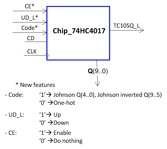 |
Fig. 2. Symbol adapted to our naming conventions and description of the chip functionality (Visio). |
Here you are some notes on specifications and planning.
Determine the execution speed. How long does it take to run a loop? And therefore, what is the maximum CLK frequency you should apply in order to make it run correctly?
2. Planning (plan X)
Fig. 3 shows an example of state diagram. This unit explains the key concept of interrupt.
We will use plan X enumerating all states.
 |
| Fig. 3. State diagram. |
You can approach the problem in successive steps. For instance:
- Step 1: plan, design and test completely a 10-bit Johnson up counter with counter enable (CE) control signal.
- Step 2: copy your previous project source files in a new folder and add the feature up/down (UD_L) to make the device reversible.
- Step 3: copy your previous project source files in a new folder and add the output combinational function to translate Johnson to one-hot code (control signal Code).
For any design step, firstly plan the hardware and secondly the software as we usually do to solve microcontroller applications.
1.- Hardware circuits and port connexions. Simply use some of the unconnected port pins available on the board to attach inputs and outputs.
2. - Software organisation. Modify the functions init_system(), output_logic(), state_logic(), read_inputs(), write_outputs(), etc. as necessary. Some notes.
RAM variables, output_logic() , state_logic() , ISR(), etc.
These Chip_74HC4017.pdsprj Chip_74HC4017.c are files to help you in this design, basically they are the project solved for a PIC16F877A: Thus an adaptation to the new target μC is required.
3. Development and 4. Testing
For any design step, compile and run Proteus and test the circuit using step by step, break points and the watch window tools. Fig. 4 show the kind of waveforms expected.
 |
| Fig. 4. Example output from Proteus logic analyser instrument (CE = 1; UD_L = 1; Code = 0) |
5. Report
Follow this rubric for writing reports.
6. Prototyping
Use training boards and perform laboratory measurements to verify how the circuit works. Fig. 5 is a picture of the project under development using the PICDEM2+ board. Using Microchip ICD2 InCircuit Debugger device you can program the HEX file or debug using the COF file, as you did in Proteus.
 |
Fig. 5. Circuit prototype mounted in a PICDEM2+ board. |
| Home Term 26/27-Q1 Contact Products Electronic devices and companies Software Books Magazines Instruments DEE Library EETAC DEEL |

|
|
| Web activa des de 09/2001, @ F. J. Robert, Web editat amb Microsoft Expression Web 4. El contingut és un complement als materials d'estudi del curs Circuits i Sistemes Digitals disponibles al campus digital Atenea. Llicència:Reconeixement 4.0 Internacional de Creative Commons |