|
|
Bachelor's Degree in Telecommunications Systems and in Network Engineering |
|
Chapter 2 problems |
- D2.4 - |
Pattern detector (FPGA-VHDL) |
V1 |
1. Specifications (Version #1)
Design phase #1: Simple FSM
Our aim is to implement a circuit to detect a given binary pattern received from a radio or wired transmitter bit stream at input T. Fig. 1 shows the symbol of this Pattern_detector circuit.
 |
|
Fig. 1. Symbol. |
The same project designed programming a µC is in D3.4.
The detected pattern is an option, for instance:
-Option #1: "0110"
-Option #2: "11010"
Use the option given by your instructor. The remaining indications in this page are adapted to the pattern in option #1.
When the sequence "0110" is detected, output Z goes high for one CLK period. Two or more adjacent patterns can also be detected as in this bit stream sequence: "01101101101..."
To make the design simpler, we will assume:
- Both, the T bitstream and the CLK are of the same frequency fCLK.
- The T bitstream signal is delayed half period (180°) with respect the CLK, to be able to sample stable data on the CLK's rising edges.
- The detector is working continuously once the power supply is turned on.
The best way to start, is to try imagining how the output will be for a given bitstream, as represented in Fig. 2.
 |
| Fig. 2. Example of timing diagram. |
2. Planning ideas to kick off the design phase #1
The planning is based on applying our FSM recipe in L6.1. This architecture is translated to VHDL as a plan C1 single file where the three main components are processes.
Draw a state diagram for the circuit's FSM. Fig. 3 shows an example, however you may imagine a different one.
 |
|
Fig. 3. Example of state diagram. States in this application represent the "memory", this is how many bits of the pattern sequence are known at a given time. Five states are required. We will assume that a CD pulse inicialises the circuit to the state zero_bits where not a single bit of the pattern is yet known. |
Adapt the FSM architecture to this problem, naming and connecting all signals and inputs and outputs.
Deduce how many D_FF are required when encoding FSM states using the following options and draw the state register memory:
Option #1: radix-2 (sequential)
Option #2: Gray
Option #3: Johnson
Option #4: one-hot
Draw the FSM state register memory block.
Write the truth table of CC2 and CC1 and their equivalent behavioural interpretations (plan B) using flowcharts.
Project location:
C:\CSD\P6\pattern_V1\(files)
Write the FSM VHDL file.
Start a Quartus Prime synthesis project for one of the following programmable target chips:
Option #1: Cyclone IV EP4CE115F29C7
Option #2: MAX II EPM2210F324C3
Option #3: MAX 10 10M50DAF484C7 (*)
(*) Remember that this chip does not generate sdo delay files, thus use another one when gate-level simulations are required.
Inspect and annotate the RTL and technology views. Check the number of D_FF synthesised in this application.
Generate a VHDL testbench fixture schematic.
Prepare a VHDL testbench fixture to adapt the stimulus signals in the Fig. 2 sketch. For driving T, it is necessary to relate time slots to the constant CLK_Period and be sure that its transitions happens away from the CLK's rising edge used for sampling.
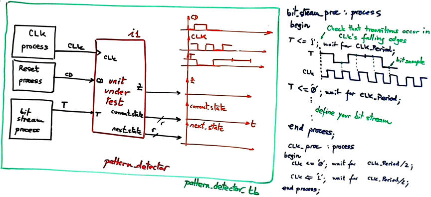 |
| Fig. 3. Example of the T process generation. |
Run functional simulations to verify your design. Visualise as well in the wave timing diagram the internal states.
Run gate-level simulations to measure the propagation time CLK to output (tCO). Measure the minimum TCLK period or the maximum frequency of operation of the FSM.
NOTE: This is cooperative group work. You must explain in the planning section of your report who is in charge of each section, who is leading the tasks, who is developing the components or sections, who is measuring or testing, etc. It is fundamental in order to obtain good assessments that you explain very well which is the contribution to the final project of each one of the group members. Besides, sections 1 and 2 are specially prepared for studying for exams. Complete all the sections 1-2-3-4-5 and write the report before attempting the next design phase. The meaning is that the basic product solved in this initial design phase must work before enhancing or complicating it with new features. Do not change the names of entities or signals already annotated. Do not copy VHDL files from anywhere (books, internet, IA, etc.); it is totally useless and penalised; your sections 3-4 will not be marked. Instead, work with the planned schematics and ask questions if necessary on how to translate them into VHDL. We can help you, remember the indications for establishing a thread of nestled Q&A using email or Meet. This full project phase will be marked as 60% of the final grade. |
Design phase #2: FSM + datapath
Add operational resources to count the numbers of times the pattern is detected in a given bitstream. After 10 pattern detections an overflow flag OV pulse resets the counter and triggers a 1.4 kHz sound wave for 1.5 s. The current number of patterns detected is also represented in a 7-segment display.
Project location: C:\CSD\P7\pattern_V1\(files)
|
NOTE: Report this design phase as an annex to the main project, reporting only what is new and what is modified from the previous design phase. This design phase will add another 20% to the final grade. |
Design phase #3: CLK_Generator
Design the CLK generator circuit from a 50 MHz quartz crystal oscillator to obtain all the clocking signals required to drive the application. We can imagine standard serial transmission frequencies as options for the bitstream.
Option #1: fCLK = 9.6 kHz
Option #2: fCLK = 38.4 kHz
Option #3: fCLK = 57.6 kHz
Deduce the number of D_FF that the full project Pattern_detector will require.
Project location: C:\CSD\P8\pattern_V1\(files)
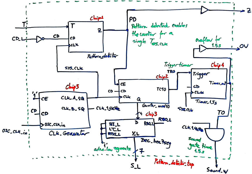
Ideas on the top design considering specifications from the three design phases imagining an FPGA prototype.
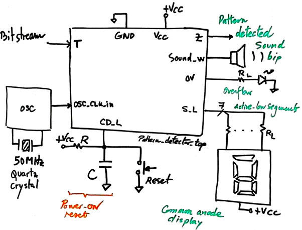
A way to start is imagining that the operational unit will also run at the same system frequency fCLK (or fSYS_CLK) used by the FSM to detect patterns.
Z pulses, signaling the detected patterns will enable counting a single event. Resetting the counter after ten events (overflow) is a synchronous operation, thus, we can invent a Counter_mod10 using the standard component Counter_mod16. The counter output TC10 will trigger the Timer_1_5s circuit that controls the sound wave gate time for TP = 1.5s and also light the OV LED.
An initial internal schematic that can let you draw a timing diagram for the signals (modify it as necessary):
You can adapt the timers from this D2.21 version A.
The circuit has a serious drawback because the T bit rate must be identical to the SYS_CLK. Why?
How we can make the bit stream rate different from the system frequency? How to modify the circuit so that it can accept several bit rates?
|
NOTE: Report this design phase as a annex, reporting only what is new and what is modified from the previous design phase. This phase will add the remaining 20% to the final grade. |
Optional: how can such circuit, in another design phase, be made programmable? The user will specify the pattern to be detected using four switches in the front panel. What kind of new hardware will be involved to detect several patterns?
Optional prototype: If such circuit has to be prototyped and experimented in the lab, how can we invent an instrument such a programmable pattern generator to be the source of the bit stream for testing and verifying our detector D2.22?
Chapter 2 problems |
- D2.4 - |
Pattern detector (FPGA-VHDL) |
V2 |
1. Specifications (Version #2)
Design phase #1: pattern detector, synchronisation and noise filtering
Our aim is to implement a circuit to detect the binary pattern P = "0110" received from a transmitter bitstream at input T. The experiment is sketched in Fig. 1.
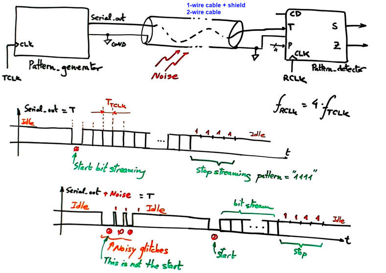 |
Fig. 1. Serial pattern generator and detector experiment. |
We can use a simple 1-wire shielded cable or a twisted-pair cable to connect the transmitter and receiver units. The pattern generator block may be like presented in D2.22. In this experiment the transmitter TCLK signal is not used, therefore we have to imagine some kind of synchronisation mechanism to allow sampling T when it is stable away from transitions. In order to adjust sampling time in the middle of each transmitted bit, the receiver RCLK frequency is four times the transmitter frequency.
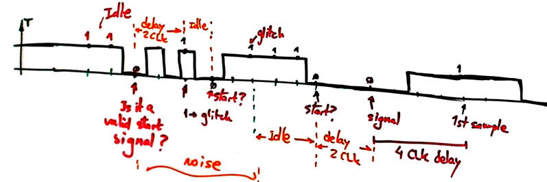
When there is no transmission, the receiver is sampling '1' and is kept idle as it is the transmitter.
The noise filter mechanism may be conceived as shown in Fig. 2: when the first '0' is detected, the receiver will wait for two RCLK to sample another value. If this new sample is '0' it is effectively the start bit of a serial transmission by the pattern generator. If this sample is '1', it means that the first '0' detected was a glitch and thus there is no transmission.
 |
| Fig. 2. Receiver signals and the idea of filtering noise. |
And the acquisition of the bit stream will consist of sampling T every four RCLK periods, as shown in Fig. 3.
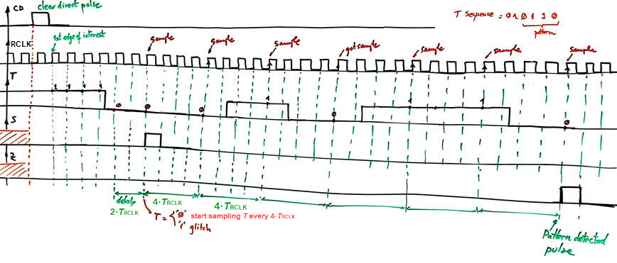 |
| Fig. 3. Receiver signals and pattern identification. |
Output S goes high for one RCLK period as a flag to indicate that bit streaming is starting.
When the pattern P = "0110" is detected output Z goes high for one RCLK period. Two or more adjacent patterns can also be detected as in this bit stream sequence: "01101101101...". We may also consider detecting anyone of the 16 different patterns, thus P indicating the code to detect is another input to the circuit.
When four '1' are detected consecutively (pattern P = "1111"), it means that the transmitter has stopped emitting or something went wrong with the bits stream and thus, the receiver must go back to idle.
2. Planning ideas to kick off the design phase #1
Several tasks have to be carried out once the start bit T = '0' is detected: synchronisation, sampling, noise filtering, data buffering, pattern comparison and detection. Those are many operations for a simple FSM as proposed above in V1; thus, it is better to conceive the system as a dedicated processor with a datapath controlled by a FSM. Fig. 4 shows a preliminary sketch of the circuit.
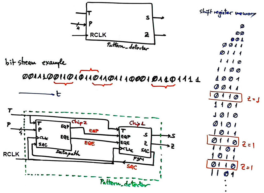 |
Fig. 4. Proposed dedicated processor. |
Fig. 5 is a detailed schematic ready for VHDL translation that includes the internal circuits of the datapath based on a shift register. Chip1 register output Q is compared to P value to generate the EQP (pattern identified) status signal. It is also compared to "1111" to generate EQE (end of streaming identified).
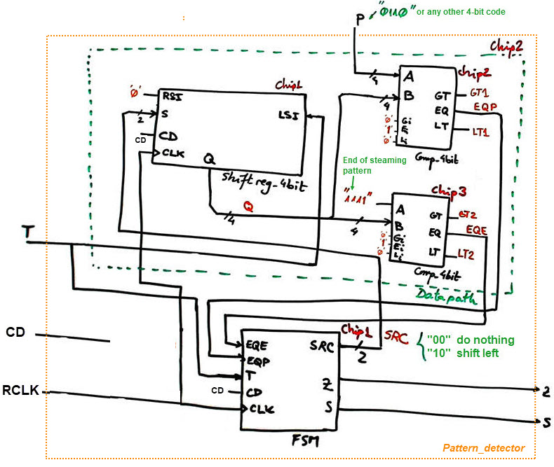 |
| Fig. 5. Proposed detailed plan for the dedicated processor and its Chip2 datapath. |
The FSM state diagram must consider delays for filtering the start bit, and additional delays for sampling T every four RCLK periods. It will generate the shift register control signals SRC to save the bit information in the shift register memory.
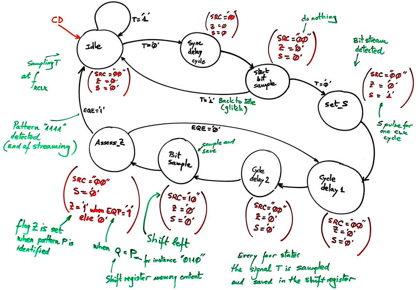 |
| Fig. 6. Initial discussion on the blocks and states that may be involved in our pattern detector. |
Draw an example timing diagram using a landscape sheet of paper with squared grid background. For instance, complete the Fig. 7.
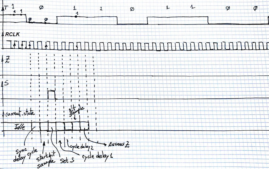 |
| Fig. 7. Example of timing diagram waveforms showing signals of interest and also states. Use a landscape paper with a squared grid background. |
Build the datapath in VHDL using plan C2 and standard components.
Adapt the FSM architecture to this problem, naming and connecting all signals and inputs and outputs.
Deduce how many D_FF are required when encoding FSM states using the following options and draw the state register memory:
Option #1: radix-2 (sequential)
Option #2: Gray
Option #3: Johnson
Option #4: one-hot
Draw the FSM state register memory block.
Write the truth table of CC2 and CC1 and their equivalent behavioural interpretations (plan B) using flowcharts.
Project location:
C:\CSD\P7\pattern_V2\(files)
Start a Quartus Prime synthesis project for one of the following programmable target chips:
Option #1: Cyclone IV EP4CE115F29C7
Option #2: MAX II EPM2210F324C3
Option #3: MAX 10 10M50DAF484C7 (*)
(*) Remember that this chip does not generate sdo delay files, thus use another one when gate-level simulations are required.
Inspect and annotate the RTL and technology views. Check the number of D_FF synthesised in this application.
Prepare a VHDL testbench fixture to adapt the stimulus signals in the Fig. 2 sketch. To translate such waveforms into a testbench process for driving T, it is necessary to rely on the constant RCLK_Period for both, generating the initial delay and implementing the bit sequence.
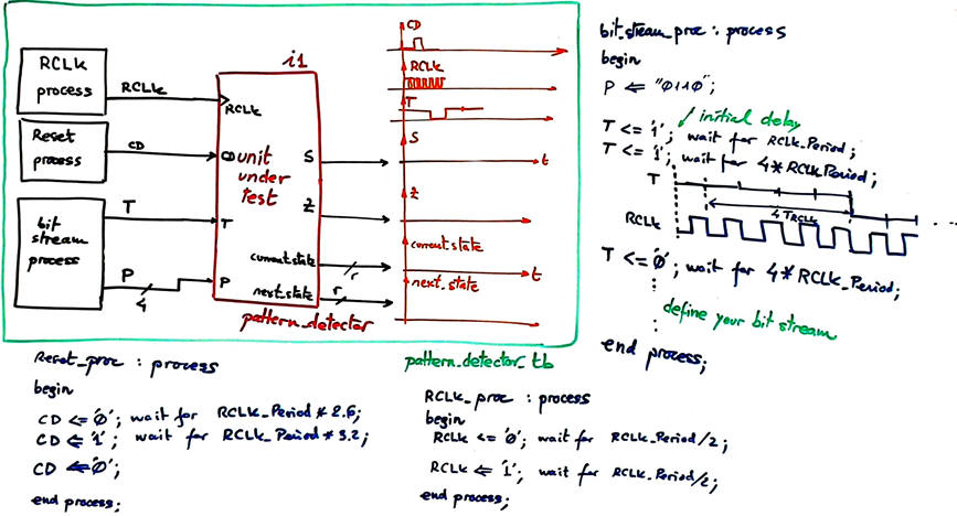 |
| Fig. 8. Example of the T process generation. |
Run functional simulations to verify your design. Visualise as well in the wave timing diagram the internal states.
Run gate-level simulations to measure the propagation time CLK to output (tCO). Measure the minimum TRCLK period or the system's maximum frequency of operation.
Design phase #2: CLK_Generator
Design the CLK generator circuit from a 50 MHz quartz crystal oscillator to obtain all the clocking signals required to drive the application. We can imagine standard serial transmission frequencies as options for the bitstream.
Option #1: fCLK = 7.2 kHz
Option #2: fCLK = 14.4 kHz
Option #3: fCLK = 38.4 kHz
Deduce the number of D_FF that the full project Pattern_detector will require.
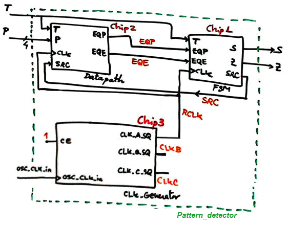 |
| Fig. 9. Pattern detector including the CLK_Generator block. |
Project location:
C:\CSD\P8\pattern_V2\(files)
Design phase #3: Counting detected events
(optional) Add operational resources to count the numbers of times the pattern is detected in a given bitstream. After 18 pattern detections an overflow flag OV pulse reset the counter and triggers a 1.4 kHz sound wave for 1.5 s. The current number of patterns detected is also represented in 7-segment displays.
| Home Term 26/27-Q1 Contact Products Electronic devices and companies Software Books Magazines Instruments DEE Library EETAC DEEL |

|
|
| Web activa des de 09/2001, @ F. J. Robert, Web editat amb Microsoft Expression Web 4. El contingut és un complement als materials d'estudi del curs Circuits i Sistemes Digitals disponibles al campus digital Atenea. Llicència:Reconeixement 4.0 Internacional de Creative Commons |