Chapter 2 problems |
- D2.2 - |
Stepper motor controller (FPGA -VHDL) |
1. Specifications
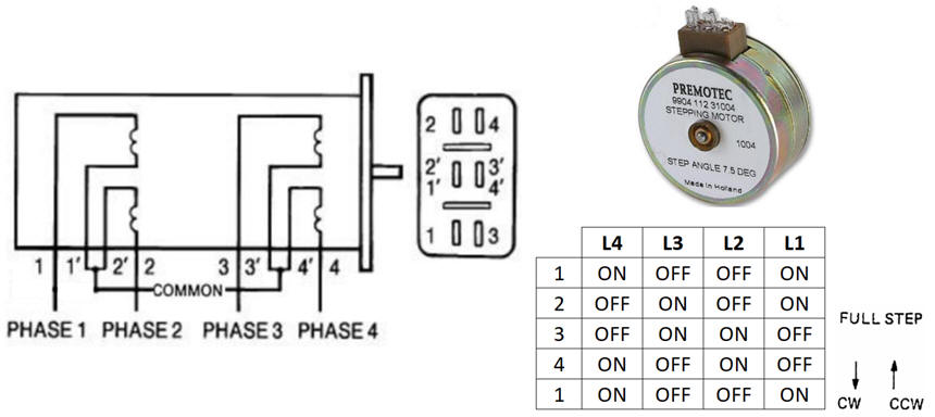
Our aim is to design the digital control unit (Stepper_cntl) for the "9904 112 31004" stepping motor from Premotec shown in Fig. 1 following our FSM strategies. Another typical stepper motor is the NEMA 17. Nowadays stepper motors can be found in computer peripherals, machine tools, medical equipment, automotive devices, or small business machines, to name a few applications. Clockwise (CW) and counter-clockwise (CCW) rotation can be achieved by reversing the step sequence. Inhibit (INH) is like a count disable, do not letting the motor rotate holding the current shaft position. Step or stride angle is 7.5 degree, thus 48 CLK periods are required for a full revolution. We can start supposing an external CLK frequency of 96 Hz, thus, when running it rotates at 2 revolutions per second.
The same project designed programming a μC is in D3.2.
To see the dynamics and connections of such motors, these are two examples of Proteus simulations:
(1) Proteus sample project using simulating the L297 stepper motor controller chip from ST.
(2) Proteus example using a microcontroller to control the stepper motor (unzip the two files in the same folder).
 |
|
Fig. 1. Example of two-phase stepper motor: characteristics, connections, full wave steeping sequence and unipolar winding. A power driver is required to energise the coils with nominal currents and voltages. |
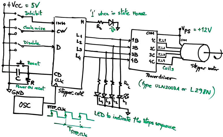
The idea is to connect four outputs to the motor coils and drive them with the right sequence so that the motor inhibits or rotates clockwise or counter-clockwise accordingly to the input signals INH and CW. We can use LED to visualise the binary sequence applied to the coils.
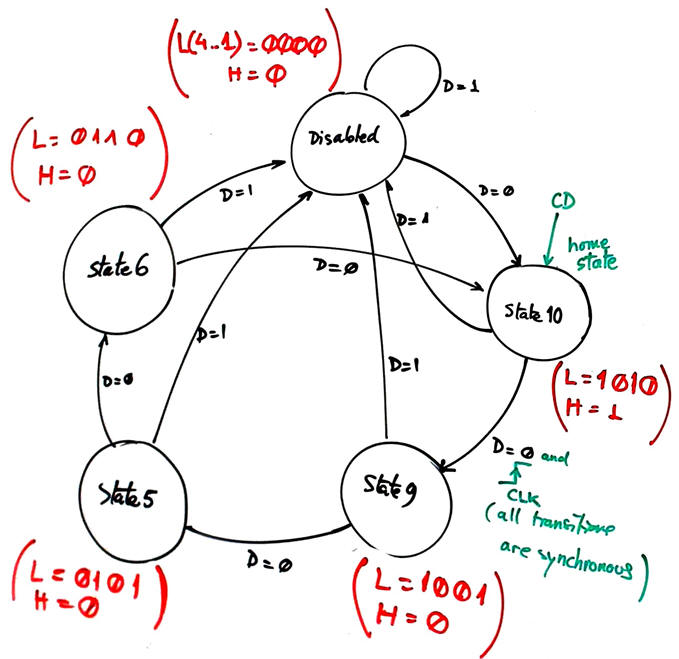
We can imagine a "disabled" state at which all coils are OFF, when switching D = '1'. The motor is not energised and thus the shaft moves freely to a given initial position before starting the motor rotation control.
The CD signal (asynchronous reset) will initialise the motor to State10 (home).
H (home) output, as in the commercial chip L297N, will be high when the controller is in State10.
 |
|
Fig. 2. Symbol and power driver inverter ULN2003A with COM = VPS. In this way, energising a coil (ON), for instance the phase 1, requires L1 = '1', P_L1 = P1' = '0'. |
2. Planning
Design phase #1: basic features. FSM architecture and current state encoding, asynchronous reset (CD), system clock (CLK), sampling input values, synchronous systems, maximum speed of operation, etc. Solve the circuit for the design step #1. This means covering P5 and P6 circuits, concepts and ideas.
Project location:
C:\CSD\P6\Stepper_cntl\(files)
- Design step #1. Consider an initial circuit to generate only the clockwise sequence and the H output. Only the switch D is required at this stage to de-energise the coils and allow the motor shaft move freely.
 |
|
Fig. 3. Symbol for the step #1. |
Draw the FSM state diagram. Fig. 4 shows an example where up to five states can be conceived to memorise the motor sequence. When the control is enabled, the sequence is generated synchronously with the CLK rising edges.
 |
|
Fig. 4. Example of FSM state diagram. |
Sketch a timing diagram showing the main operations and also imagining state values. These stimulus signals can be applied in section fourth in the testbench process translated to VHDL.
 |
|
Fig. 5. Timing diagram example. |
Adapt the FSM architecture to this problem, naming and connecting all signals and inputs and outputs. This will be translated as a single plan C1 VHDL file. Deduce how many D_FF are required when encoding FSM states using the following options and draw the state register memory:
Option #1: Radix-2 (sequential)
Option #2: Gray
Option #3: Johnson
Option #4: One-hot
 |
|
Fig. 6. FSM adaptation to the problem. |
Write the CC2 truth table to obtain the outputs of the circuit and its flowchart.
 |
|
Fig. 7. CC2 truth table and its equivalent plan B flowchart ready for VHDL translation. |
Design the CC1 truth table to obtain the next state to go and its flowchart.
 |
|
Fig. 8. CC1 truth table and its equivalent plan B flowchart ready for VHDL translation. |
3. Development
Write the VHDL file.
Start a Quartus Prime synthesis project for one of the following programmable target chips:
Option #1: Cyclone IV EP4CE115F29C7
Option #2: MAX II EPM2210F324C3
Option #3: MAX 10 10M50DAF484C7 (for gate-level simulations, choose one of the previous options)
Inspect and discuss the RTL and technology schematics. Check the number of D_FF.
 |
|
Fig. 9. RTL schematic generated by Quartus Prime and project summary where we can check the resources used and the number of D_FF. |
 |
|
Fig. 10. Technology view where we can indicate and count the number of D_FF of the state register. |
4. Testing functional
Draw the testbench fixture, add stimulus processes to the VHDL template and run the EDA simulation tool to verify your design. Discuss your results on the wave pictures.
 |
|
Fig. 11. Testbench fixture schematic for the basic FSM in step #1. |
 |
|
Fig. 12. Waveforms showing the full cycle of signals and internal states of the automata. |
5. Testing (gate-level)
Measure the maximum CLK frequency related to tCO that can be applied to your design considering your target chip.
 |
|
Fig.13. Example of gate-level simulation to measure the propagation time from CLK to output (tCO). |
Go ahead with the step #2 only when step #1 is fully tested working correctly.
- Design step #2. Add the inhibit (INH) and also the CW control signals to the basic FSM.
Go ahead with the step #2 only when step #1 is fully tested working correctly and its report is written. Explain how the new symbol will look like, use a dotted box as usual in CSD, what are the modifications for the new features, new inputs and outputs. What components will contain the datapath. Etc.
Only when design phase #1 is fully tested working correctly and reported, solve the design phase #2 as advancing to cover P7 and P8 materials. Project location:
Design phase #2: dedicated processor, real-time, advanced features.
- Design step #1: Design a CLK generator to obtain all the necessary CLK signals from the target board quartz crystal oscillator (50 MHz). Deduce the number of D_FF required for this subcircuit.
Project location:
C:\CSD\P8\Stepper_cntl\(files)
- Design step #2. Let us attach to the controller a tachometer o revolutions per minute (RPM) meter. If CW = '1' the internal counter will increment when detecting the HOME signal. If CW = '0' it will decrement when detecting the HOME signal.
Project location:
C:\CSD\P7\Stepper_cntl\(files)
- Design step #3. The stepper_cntl rotating speed may be programmable using an 8-bit data input S(7..0). Discuss how to implement such enhancement: a programmable speed generator. What may be the maximum speed of rotation for a given commercial stepper motor?
Additional materials, references and ideas on stepper motors:
- Stepper motor position control. How to establish a starting "home" position. Using a microswitch or an optical detector. Rotary encoder for position feedback.
- How to calculate rpm of stepper motor?
- How to generate the several coil control sequences: normal drive, wave drive and half step?
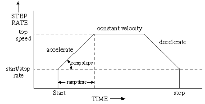
- Trapezoidal velocity profile: start/stop rate, accelerate, nominal speed, decelerate (Dover ref.). If the stepper motor is required to move a heavy load it will normally be necessary to start the movement slowly (as with any motor) and accelerate to the desired speed and, equally, to decelerate when it is necessary to stop.

- Stepper Motor Calculations (ref.).
- Stepper motor basics (ref.)
Hint: Suggested report organisation (similarly for slides presentation)
1. Specifications. First you explain all the specifications you like for your product. Add theory about anything of interest if necessary to comprehend the application.
2. Plan. Here you say that you have in mind several design phases and steps, each time incorporating only a few new features. And thus, that you simply will start developing and testing only what you have planned to be the first step.
3. Develop only the first step of the design phase #1
4. Test only the first step of the design phase #1
Annexes.
- Phase #1, step #2 (inhibit and rotation direction) Explain and do only what is modified in each of the previous sections to introduce the new features.
- Phase #2, step #1 (CLK_Generator) Explain and do only what is modified in each of the previous sections to introduce the new features. etc.


