|
|
Bachelor's Degree in Telecommunications Systems and in Network Engineering |
|
|
|
||
|
|
Bicycle flashing lamp with a single push-button |
|
|
|
||
Basics on synchronous FSM
| 1. Specifications | Planning | Developing | Test functional | Test gate-level | Report | Prototype |
Let us design a flashing lamp like the one represented in Fig.1 similar to the torches used in bikes. This is the FSM design approach targeting a programmable device like a CPLD or a FPGA for prototyping.
- First click: LED on.
- Second click: LED blinking at 5 Hz frequency.
- Third click: all LED off.
Additional ideas may be modulating LED light intensity and save energy switching off the lamp after some minutes of inactivity.
 |
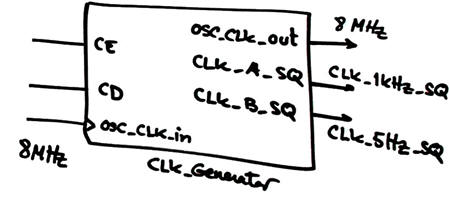
Fig. 1. Example of a commercial LED flashing torch for a bicycle and internal blocks proposed. Blinking mode of operation is attained using a 5 Hz square wave selected by the multiplexer MUX_4. It is acting as a very simple datapath selecting which data is driving the LED lamp. In a new design phase we can invent the Chip3 CLK_generator required to obtain the CLK_1kHz_SQ and CLK_5Hz_SQ signals from an external high frequency oscillator. |
 |
|
The idea of power-on reset or clear direct (CD) clicks are depicted in Fig. 2. More ideas on this concepts are available in Power_on unit.
 |
|
Fig. 2. The idea of power on reset and CD clicks to initialise the system. |
SSketch a timing diagram showing the main operations and also imagining state values. These stimulus signals can be applied in section fourth in the testbench process translated to VHDL. Fig. 3 shows an example timing diagram.
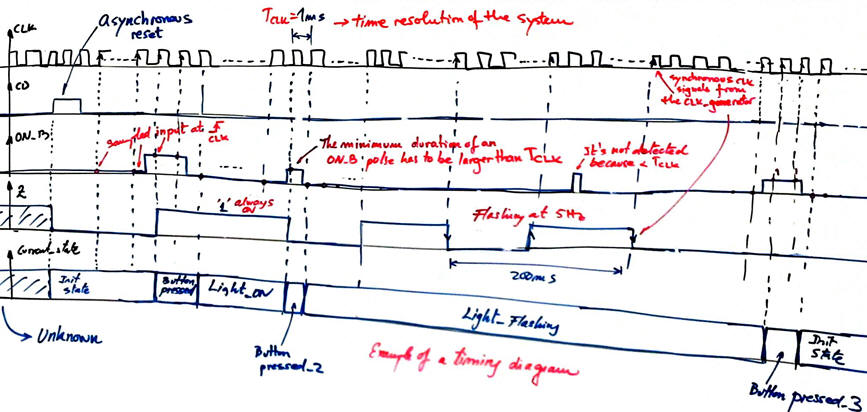 |
| Fig. 3. Example timing diagram imagining internal states. |
| Specifications | 2. Planning | Developing | Test functional | Test gate-level | Report | Prototype |
Design phase #1: basic features. FSM architecture and current state encoding, asynchronous reset (CD), system clock (CLK), sampling input values, synchronous systems, maximum speed of operation, etc. This means covering P5 and P6 circuits, concepts and ideas. CLk will be a squared signal of 1 kHz.
- Step #1: FSM
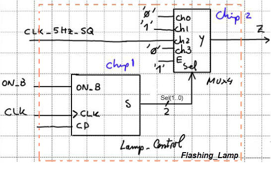 |
Fig. 4. The proposed circuit based on a synchronous FSM that is driving the MUX_4 selector signals. Chip2 MUX_4 selects ON ('1'), OFF ('0') or intermittency (5 Hz). New light signals can be easily added in other channels. |
Project location:
C:\CSD\P6\Flashing_lamp\(files)
The project will contain 3 VHDL files, the top entity Flashing_Lamp, and the two internal components: MUX4 and Lamp_control..
Let us infer the state diagram so that the system has enough internal memory to remember the three consecutive clicks from the the same push-button ON_B. As you see in Fig 5, up to 6 states are required.
 |
| Fig. 5. State diagram for this application. |
Adapt the FSM architecture to this problem, naming and connecting all signals and inputs and outputs. This will be translated as a single plan C1 VHDL file. Deduce how many D_FF are required when encoding FSM states using the following options and draw the state register memory:
Option #1: Radix-2 (sequential)
Option #2: Gray
Option #3: Johnson
Option #4: One-hot
 |
|
Fig. 6. FSM adaptation to the problem and state register composition using a number r of D_FF depending on the internal states encoding option. |
Write the CC2 truth table to obtain the outputs of the circuit and its flowchart.
 |
|
Fig. 7. CC2 truth table and its equivalent plan B flowchart ready for VHDL translation. |
Design the CC1 truth table to obtain the next state to go and its flowchart.
 |
|
Fig. 8. CC1 truth table and its equivalent plan B flowchart ready for VHDL translation. |
- Step #2: Modulate the LED light intensity
For instance, imagine a new operating mode when clicking ON_B for the third time: LED lighting at haft power intensity by means of a 500 Hz 50% duty cycle waveform.
| Specifications | Planning | 3. Developing | Test functional | Test gate-level | Report | Prototype |
Let us use the AMD (Xilinx) CPLD XC2C256-TQ144-7 that populates the CoolRunner-II CPLD Starter Board. To develop this application Xilinx ISE software is required. It still can be installed using a virtual machine running Windows 7.
VHDL files translated form above flowcharts. It is a plan C2 design consisting in two flies: top entity Flashing_Lamp.vhd, MUX4.vhd from a previous project in P2, and Lamp_Control.vhd that contains the FSM in a single file in plan_C1.
Project name is Flashing_Lamp_prj and the project location is:
C:/CSD/P6/Flashing_Lamp/(files)
Let's see if the EDA tool synthesiser interprets correctly the high-level (behavioural) FSM descriptions producing the RTL picture in Fig. 9.
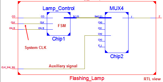 |
Fig. 9. The RTL schematic. |
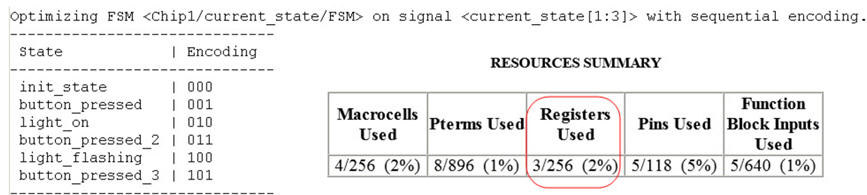
Check the binary code in which the FSM is encoded and the number of 1-bit memory registers used (DFF). Here in Fig 10. there is a detailed RTL view of the FSM that contain all the registers. Using a binary "sequential" encoding, 3 DFF can hold up to 8 states.
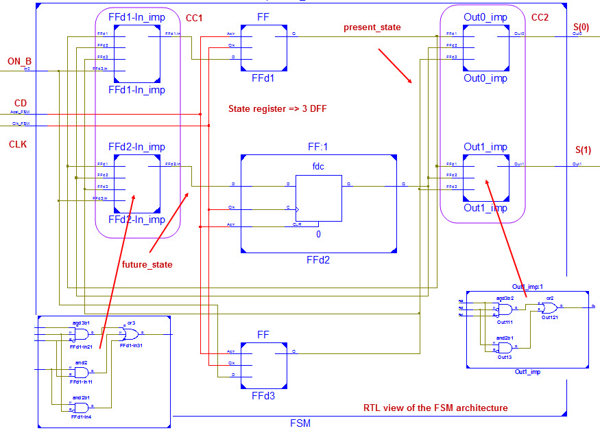 |
Fig. 10. Number of registers used in the synthesis of the circuit. |
This is the report text file where the FSM encoding can be seen:
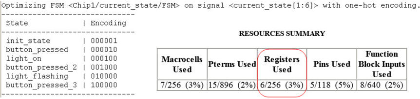
Alternatively, it is possible to change the FSM encoding parameter to for instance "one-hot" (6 registers).
| Specifications | Planning | Developing | 4. Test functional | Test gate-level | Report | Prototype |
This in Fig. 11 is the VHDL testbench schematic that we have in mind to run simulations for synchronous circuits.
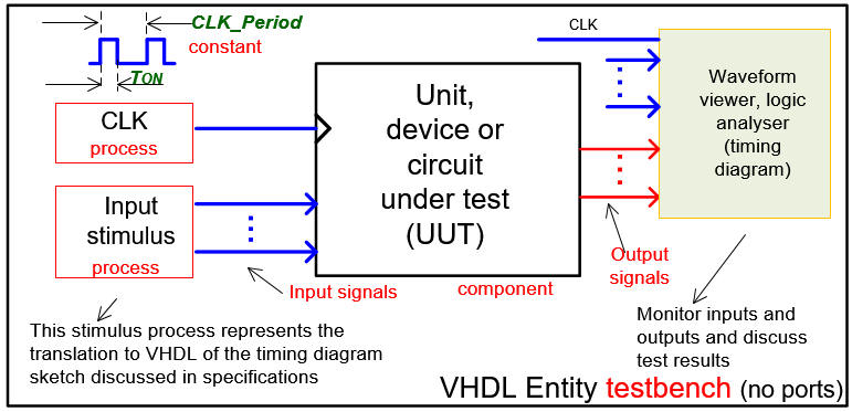 |
| Fig. 11. Testbench where to make it easy the CLK is another concurrent process. (visio) |
This is a sample test bench file Flashing_Lamp_tb.vhd. Run the EDA VHDL tool and demonstrate how the circuit works adding comments to the printed sheet of paper containing the waveforms. Naturally, signals of very different frequencies such 5 Hz and 1 kHz, cannot be represented correctly in a full view in a single time scale.
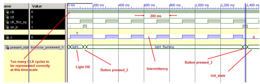 |
Fig. 12. Example of a timing diagram to show how the circuit works. |
Therefore, to see how the system sample ON_B values at the rising edge of the CLK, you have to zoom as in Fig. 13.
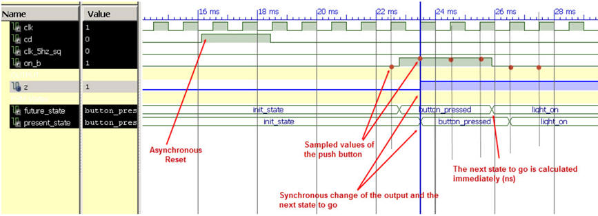 |
Fig. 13. Zoom at the system CLK scale to observe the synchronicity. |
| Specifications | Planning | Developing | Test functional | 5. Test gate-level | Report | Prototype |
Gate-level simulations in ISIM.
 |
|
Fig. 14. Zooming in a signal transition we can measure the propagation time from CLK to output Z (tCO). |
Xilinx ISE timing analyser
|
|
|
Fig. 15. Using the spreadsheet we can determine the maximum frequency of operation repeating and automating in some way the measurement in Fig. 14. |
| Specifications | Planning | Developing | Test functional | Test gate-level | 6. Report | Prototype |
Follow this rubric for writing reports.
| Specifications | Planning | Developing | Test functional | Test gate-level | Report | 7. Prototype |
Once the circuit works in design phase #1 project and has been reported, the idea is to continue the project development in the laboratory downloading the configuration file into a given CPLD or FPGA. In our lab, there are several training boards, for instance the Digilent Coolrunner which is populated with a CPLD XC2C256-TQ144-7. Thus, it is time to verify how the circuit works in real and use the instrumentation to make measurements.
Design phase #2: Advanced features: CLK generation, real-time timing, prototiping, etc.
- Step #1: CLK_Generator and prototyping.
Project location:
C:\CSD\P8\Flashing_lamp\(files)
Specifications. To complete the schematic in Fig. 1, the CLK_generator is required to obtain CLK_1kHz_SQ and CLK_5Hz_SQ from the board's 8 MHz main quartz oscillator.
 |
|
Fig. 16. CLK_Generator synbol. The input OSC_CLK_in is buffered as OSC_CLK_out for debugging purposes. |
Planning. The CLK_Generator internal design is based on chaining Freq_divN and D_FF to obtain 1 kHz and 5 Hz.
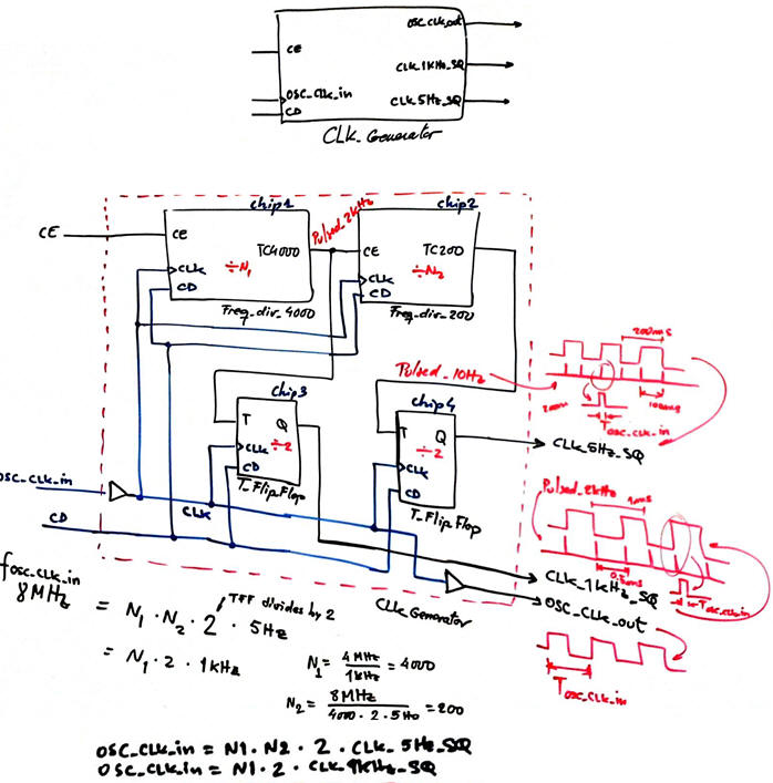 |
| Fig. 17. Proposed generic modular architecture for designing CLK_Generator. |
Where for instance Freq_div_4000 and Freq_div_200 are easily adapted using plan Y adjusting the number of states and size of vector signals.
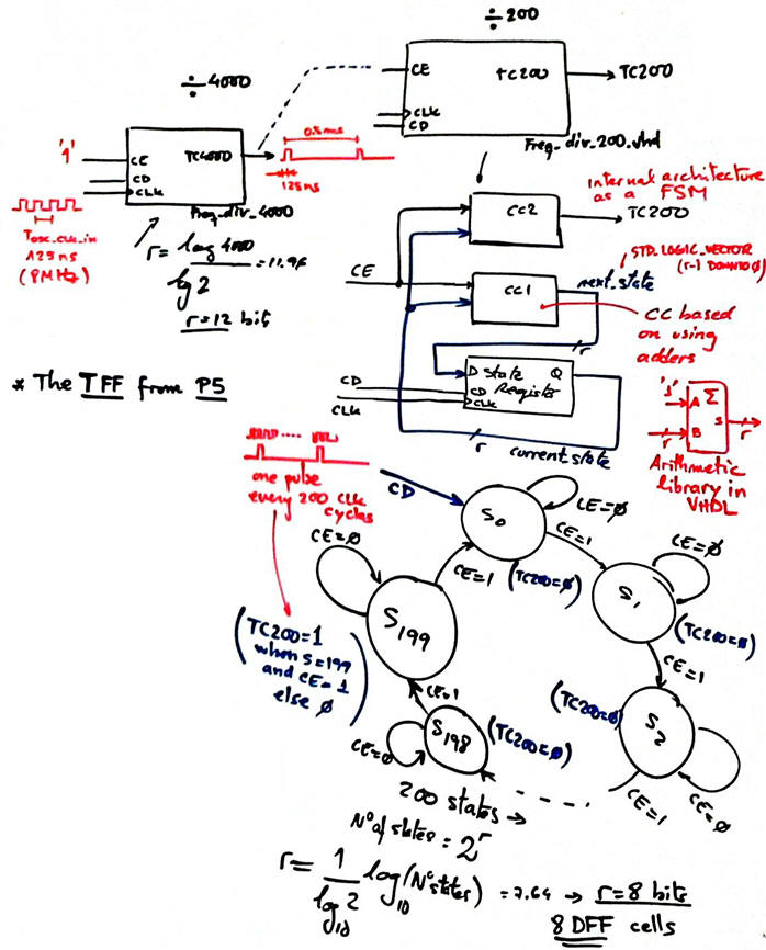 |
| Fig.18. Plan Y design of the Freq_div_4000 and Freq_div_200. |
Development. Synthesising the application circuit generates an RTL as follows:
 |
| Fig. 19. RTL view of the full project. |
Optional. Explain how to speed up a CLK_Generator testbench when a large amount of time simulation is required. What is the way to shorten the simulation time keeping the circuit structure?
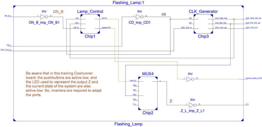
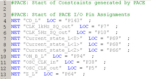
Testing and prototyping. The pin assignment file (ucf) is easily produced using the spreadsheet in ISE as indicated in Fig. 20. The board's datasheet indicates as well the three LED used for debugging purposes to show the current_state vector value.
 |
| Fig. 20. Pin assignment. |
This is the list of all the source files to complete this project. Fig. 21 is a picture of the board running.
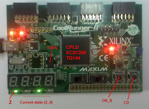 |
Fig. 21. The prototyping board populated with a Xilinx Coolrunner CPLD. |
This is a video showing the sequence of operations triggered when pressing the ON_B.
This is the flashing lamp using a DE2-115 board from Intel and Cyclone IV FPGA.
- Step #2: Automatic switch off
Save energy turning off the lamp after 3 minutes of inactivity.
As shown in Fig. 22, this new interesting feature means designing and activating an electronic power load switch such the TI TPS22950 or the Torex XC6193 to apply VCC power to the Flashing_lamp controller. The idea is to replace the traditional mechanical switch by this smart push-button.
What kind of circuit may include the P-MOSFET gate control? Basically a 1-bit memory cell type RS_Latch from L5.1 adapting the active-levels of the control inputs set and reset. Let us imagine that the ON push-button is active-low and the shutdown signal is active-high.
 |
| Fig. 22. Example of push-button switch or voltage-controlled switch activated by clicking the ON pushbutton and turn off when the application sends a shutdown pulse. Commercial circuit such Torex XC193 include additional features such as turn on and turn off delay times, current limiting, short-circuit and over-temperature protection. |
This is an example of simulation of the basic load_switch.pdsprj in Proteus. We can mount a prototype soldering the IRF9530 power PMOS and the 4011 chip in an universal board.
 |
| Fig. 23. Example of basic push-button load switch activated by clicking the ON_L pushbutton and turned off when the application sends a SHDN pulse after finishing operation. In this way the battery remains disconnected from the application. |
We can mount a prototype soldering the IRF9530 power PMOS and the 4011 chip in an universal board.
|
|
| Fig. 24. Example of load switch prototype caracterised driving the circuit and measuring using y the VB8012 instrument. |
| Home Term 26/27-Q1 Contact Products Electronic devices and companies Software Books Magazines Instruments DEE Library EETAC DEEL |

|
|
| Web activa des de 09/2001, @ F. J. Robert, Web editat amb Microsoft Expression Web 4. El contingut és un complement als materials d'estudi del curs Circuits i Sistemes Digitals disponibles al campus digital Atenea. Llicència:Reconeixement 4.0 Internacional de Creative Commons |