|
|
Bachelor's Degree in Telecommunications Systems and in Network Engineering |
|
(A) Synchronous shift registers, (B) Barrel p_shift registers |
Standard sequential components
| 1. Specifications | Planning | Developing | Testing (functional) | Testing (gate-level) | Prototype | Report |
Fig. 1 shows the symbol of the shift register circuit to be designed. This is the classic chip 4-bit shift register 74HCT194. Two strategies are possible when imagining size n-bit: plan Y and plan C2, and thus we propose to compare them.
Let us start designing a 4-bit shift register using plan Y.
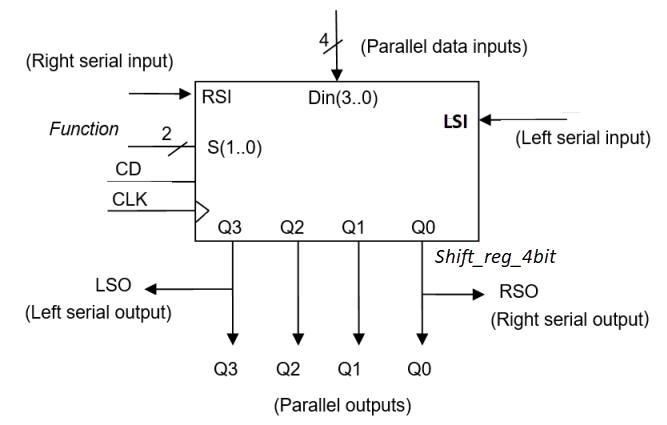 |
Fig 1. Symbol for a 4-bit shift register. |
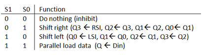 |
Fig 2. Function table indicating the four modes of synchronous operation. When S = S(1) = S(0) = LD = "00" or "11", thus connecting both control signals together, the circuit becomes a Data_reg_4bit. |
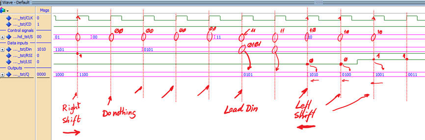
The four modes of operation can be better comprehended studying an example of timing diagram like in Fig. 3.
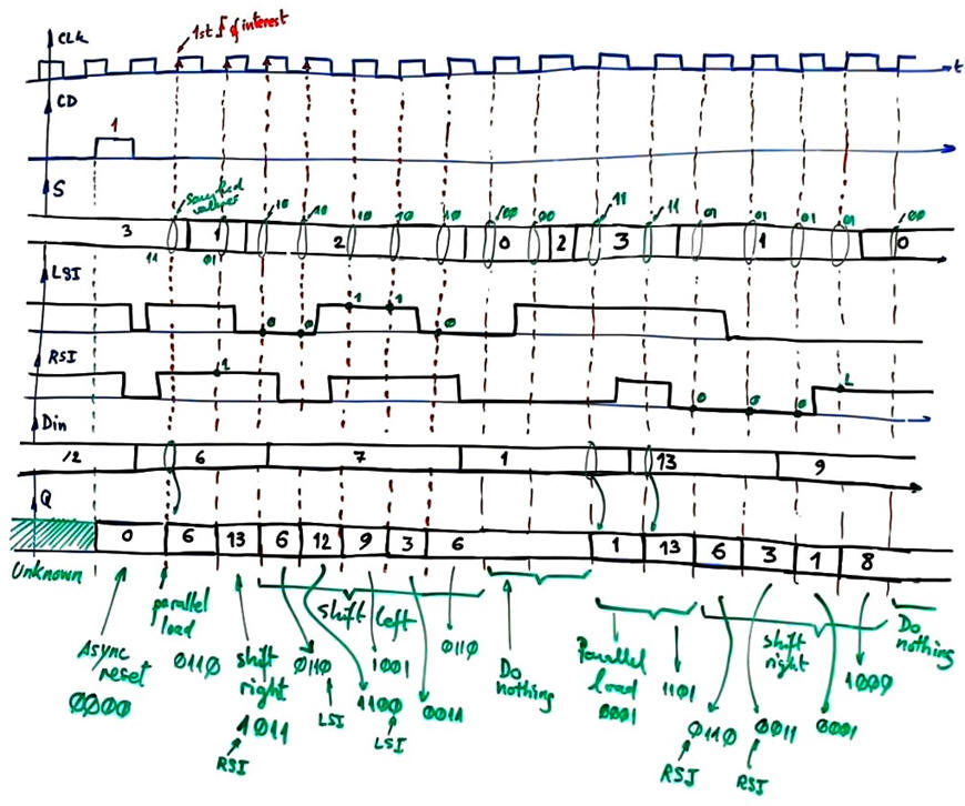 |
| Fig. 3. Example of timing diagram. |
| Specifications | 2. Planning | Developing | Testing (functional) | Testing (gate-level) | Prototype | Report |
The state diagram cannot be represented for all 16 states; it is a flexible circuit that as shown in Fig. 4, from each state it is possible to jump to many other states, representing 336 state transitions.
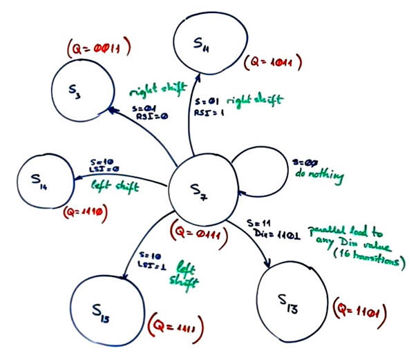 |
Fig 4. Example state diagram representing state transitions for a given state. Shift registers are extremely versatile devices., allowing to jump from any state to to any other one. |
Sixteen states and hundreds of state transitions makes this circuit specially adequate for plan Y, encoding internal states as STD_LOGIC_VECTOR in binary radix-2.
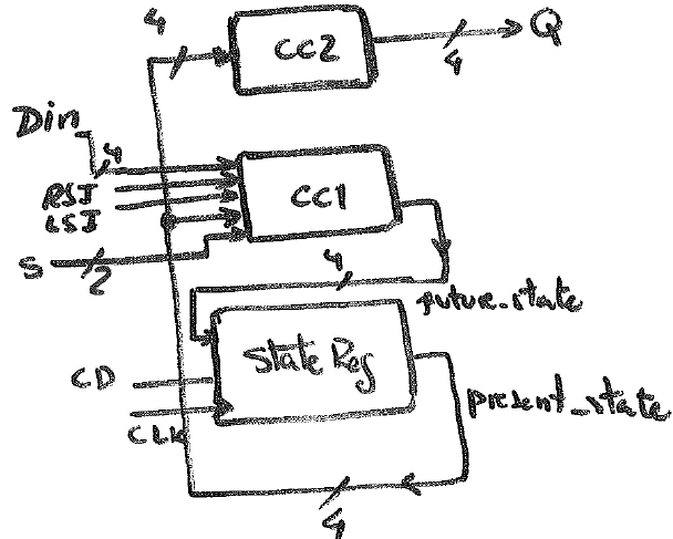 |
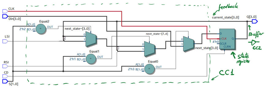
Fig 5. FSM adaptation. When using plan Y, the CC2 circuit is simply a buffered copy of the present_state internal signal. |
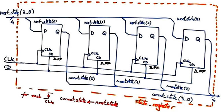
State register is composed as usual by four D_FF working synchronously in parallel.
 |
|
Fig. 6. State register consist of four D_FF working synchronously in parallel. |
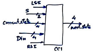
CC1 is a complex function of 4096 combinations. Using the S(1..0) control signal it can be subdivided in four sections. Fig. 7 represents the CC1 flowchart ready for VHDL translation.
 |
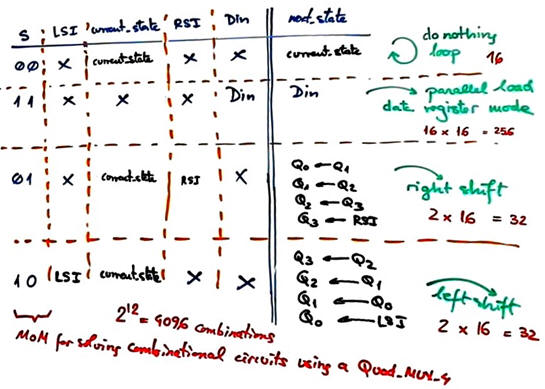 |
Fig. 7. Example of CC1 truth table representing the 4096 combinations. We can count the 336 state transitions counted in Fig. 4. |
|
An example of RTL that can be deduced for such CC1 truth table is represented in Fig. 8 using the MoM and a Quad_MUX_4. However, we better describe the truth table using a behavioural plan B approach, as represented in Fig. 9. The advantage is that it is easily translated in VHDL using a process, thus keeping all the sequential FSM in a single file (plan C1).
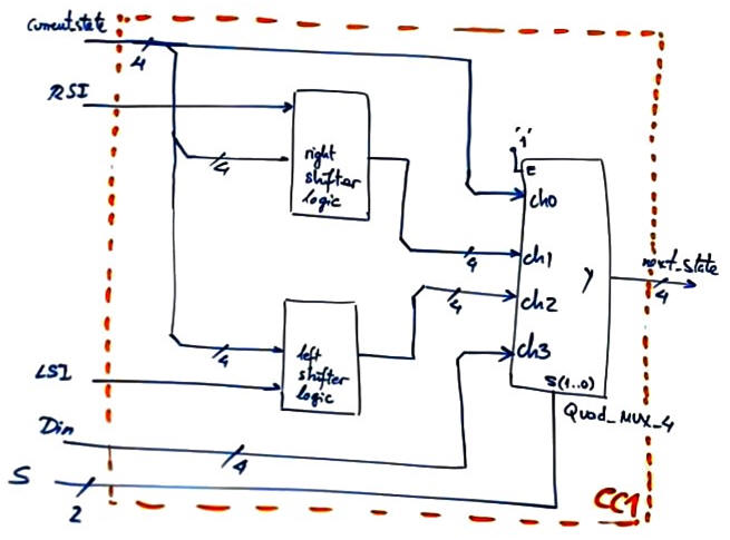 |
| Fig. 8. Example of elaboration of CC1 using the method of multiplexers and a Quad_MUX_4. |
Fig. 9 is the behavioural interpretation of the CC1 truth table using a convenient flowchart.
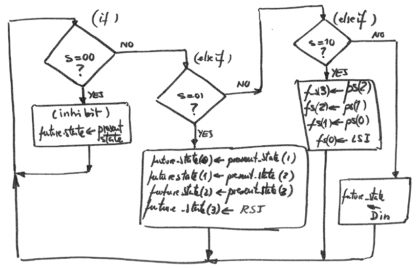  |
| Fig. 9. CC1 flowchart. |
Project location:
C:\CSD\P7\Shift_reg_4bit\(files)
Discussion on building larger shift registers:
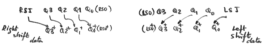
- How to invent a Shift_reg_16bit using plan Y? Adjust the size of STD_LOGIC_VECTOR state signals to n bits and apply in CC1 the same flowchart in Fig. 9 shifting the n bits in successive bit operations.
- How to invent Shift_reg_14bit using plan C2? This is chip expansion using standard components like Shift_reg_4bit and Shift_reg_2bit. Fig. 10 shown the schematic. RSI and RSO (and LSI and LSO) signals are easily chainable to the desired register size. This is a three VHDL file project.
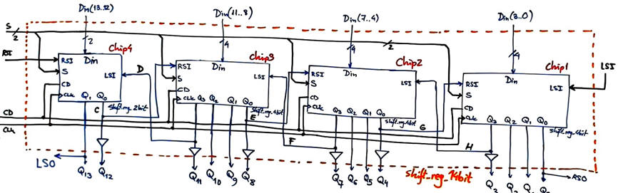 |
| Fig. 10. Shift_register_14bit schematic using plan C2. |
| Specifications | Planning | 3. Developing | Testing (functional) | Testing (gate-level) | Prototype | Report |
Translate to VHDL using a single file plan C1 the FSM in Fig. 5. This is an example VHDL file Shift_reg_4bit.vhd. State signals are STD_LOGIC_VECTOR (plan Y), making it simple expanding the circuit to a larger n number of bits.
RTL schematic.
 |
| Fig. 11. RTL schematic. |
Technology view shows that the implementation uses four D_FF as expected.
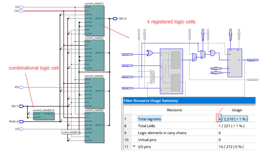 |
| Fig. 12. Technology view when synthesising for an Intel MAX II device. |
| Specifications | Planning | Developing | 4. Testing (functional) | Testing (gate-level) | Prototype | Report |
The VHDL testbench fixture will apply input stimulus to the unit under test. Our idea is to verify that the circuit works ideally as presented in Fig. 3 timing diagram.
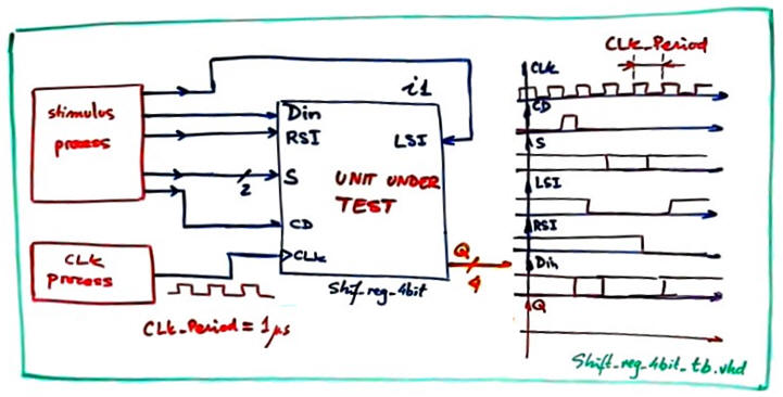 |
| Fig. 13. VHDL testbench idea. |
Generate the testbench skeleton and prepare both CLK and stimulus processes.
This is an example Shift_reg_4bit_tb.vhd file from which to copy the stimulus processes and the constant CLK_Period that determines time resolution.
Print and discuss, as in Fig. 14, wave diagrams showing how the circuit evolves in time accordingly to the modes of operations selected with the control input vector S.
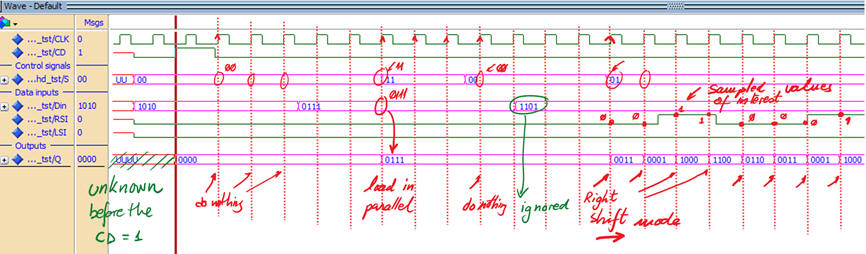  |
| Fig. 14. Functional results. |
| Specifications | Planning | Developing | Testing (functional) | 5. Testing (gate level) | Report | Prototype |
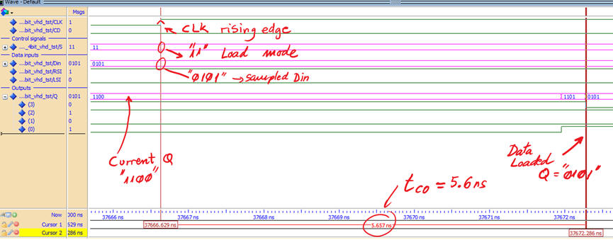
Example of tCO measurement. Din = "0101" is sampled at the rising edge when the mode of operation is parallel load S = "11". For this MAX II device it takes 5.6 ns to carry out this order to settle the outputs at the new sampled value.
 |
| Fig. 15. Measuring tCO in a given transition. |
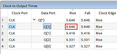
The worst-case scenario will be calculated by the Quartus Prime timing analyser tool, as shown in Fig. 16. tCO = 5.65 ns. It means that we can sped up CLK signal up to fMAX = 177 MHz, implying that for this particular target chip we can run 177 millions of synchronous load and shift operations per second.
 |
| Fig. 16. Timing analysis spreadsheet from which to calculate the maximum frequency of operation. |
| Specifications | Planning | Developing | Testing (functional) | Testing (gate-level) | 6. Prototype | Report |
Use training boards such the DE10-Lite and perform laboratory measurements to verify how the circuit works. Shift registers are the key components in serial transmissions as shown in this USART project. It is also the key component in all kind of information panels where the characters are shifted, and also in many electronic toys or gambling systems (roulette D2.12)) or Christmas tree illumination systems where LED patterns are dynamically shifted to represent a variety of light shapes and patterns.
| Specifications | Planning | Developing | Testing (functional) | Testing (gate-level) | Prototype | 7. Report |
Follow this rubric for writing reports.
(A) Synchronous shift registers, (B) Barrel p_shift registers |
| 1. Specifications | Planning | Developing | Testing (functional) | Testing (gate-level) | Prototype | Report |
Let us invent a 21-bit barrel 3_shift register as shown in Fig. 1, a device capable of shifting 3-bit in a single CLK period. This device is a generalised version of the standard shift register. The assignment D1.9 shows the combinational version of this component. In a first step, we fix the number of bits to shift per CLK cycle to 3.
Thus, in a second step, if required, we can make the device more flexible adding the control input P to establish the number of bits to shift.
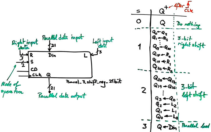 |
| Fig. 1. Symbol for the barrel 3_shift register of 21-bit. |
| Specifications | 2. Planning | Developing | Testing (functional) | Testing (gate-level) | Prototype | Report |
We will use plan Y because it is the most efficient way to translate the function table for this FSM. It is easily adaptable to any vector size n-bit or to any number of p-shift bits.
Project location:
C:\CSD\P7\Barrel_3_shift_reg_21bit\(files)
| Specifications | Planning | 3. Developing | Testing (functional) | Testing (gate-level) | Prototype | Report |
| Specifications | Planning | Developing | 4. Testing (functional) | Testing (gate-level) | Prototype | Report |
Barrel_3_shift_reg_21bit_tb.vhd
Barrel_3_shift_reg_21bit_wave.do ModelSim waves signal setup.
| Specifications | Planning | Developing | Testing (functional) | 5. Testing (gate level) | Report | Prototype |
| Specifications | Planning | Developing | Testing (functional) | Testing (gate-level) | 6. Prototype | Report |
An example prototype for the legacy DE0 board from Terasic company populated with the Intel Cyclone III 3C16F484C6N FPGA is explained in this page Barrel_3_shift_reg_21bit.
| Specifications | Planning | Developing | Testing (functional) | Testing (gate-level) | Prototype | 7. Report |
| Home Term 26/27-Q1 Contact Products Electronic devices and companies Software Books Magazines Instruments DEE Library EETAC DEEL |

|
|
| Web activa des de 09/2001, @ F. J. Robert, Web editat amb Microsoft Expression Web 4. El contingut és un complement als materials d'estudi del curs Circuits i Sistemes Digitals disponibles al campus digital Atenea. Llicència:Reconeixement 4.0 Internacional de Creative Commons |