|
|
Bachelor's Degree in Telecommunications Systems and in Network Engineering |
|
P5: analysis of circuits based on flip-flops, latches and logic gates |
| Resources in lectures and labs: | L5.1, L5.2, L5.3,L5.4 | Project | objectives |
Highlighted project: asynchronous circuit based on flip-flops
| Method I | Method II | Method III |
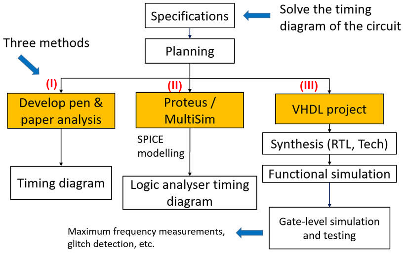
As shown in P1, analysis projects consist of four sections following the sequence represented in Fig. 1.
 |
| Fig. 1. Organise your analysis project following this sequence. Write your report only when your result is verified using another analysis method. |
And Fig. 2 explain the main details of each analysis method.
 |
|
Fig. 2. We get solutions determining how the circuit works comparing results form three methods. Be aware that each method is planned in small successive steps. |
These are other tutorials and assignments.
| Top | Circuit_async2 method I | Method II | Method III |
| 1. Specifications | Planning | Developing | Testing | Report |
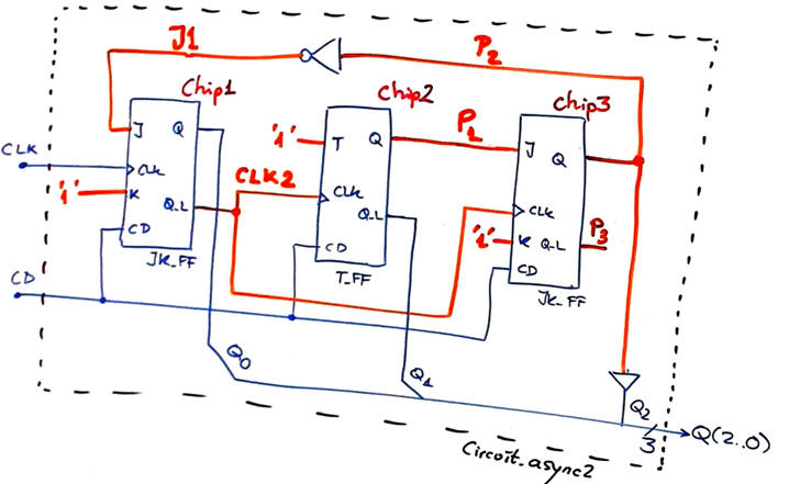
Analyse Circuit_async2 represented in Fig. 3 based on flip-flops using a handwriting analysis method I. Answer these questions:
- Obtain the timing diagram.
- Determine what kind of output codes Q(2..0) are generated in each CLK cycle.
- What is the function of this circuit?
- Measure propagation delays CLK to output (tCO) and deduce the maximum CLK frequency fCLK_max that can be applied to the circuit.
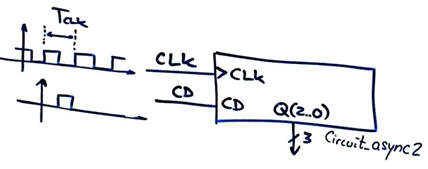 |
Fig. 3. Symbol and schematic of the asynchronous circuit to be analysed. CLK is a rectangular wave of TCLK period. Clear direct (CD) is a single pulse any time the user likes to initialise the circuit. |
 |
|
| Specifications | 2. Planning | Developing | Testing | Report |
Pictures, notes, scanned materials, theory, etc. can be stored in this project location:
C:\CSD\P5\Circuit_async2\paper\(files)
General procedure and paper work for analysing circuits based on flip-flops. Identify the number of CLK signals in the circuit. Is it asynchronous or synchronous?
Step #1: Study how a single FF works. Imagine values for control input T (or D, JK, RS) and try to obtain outputs applying function tables. On these pages there are T_FF and JK_FF circuits.
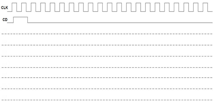
Step #2: If asynchronous, solve a circuit with two CLK signals. To draw the timing diagram, go advancing in time by TCLK periods (circuit's time resolution). Apply an initial CD pulse to reset the system and start from a known state.
This is a video rec. that explains the problem planning and solutions, the last part of which shows how to deduce the timing diagram in paper.
 |
|
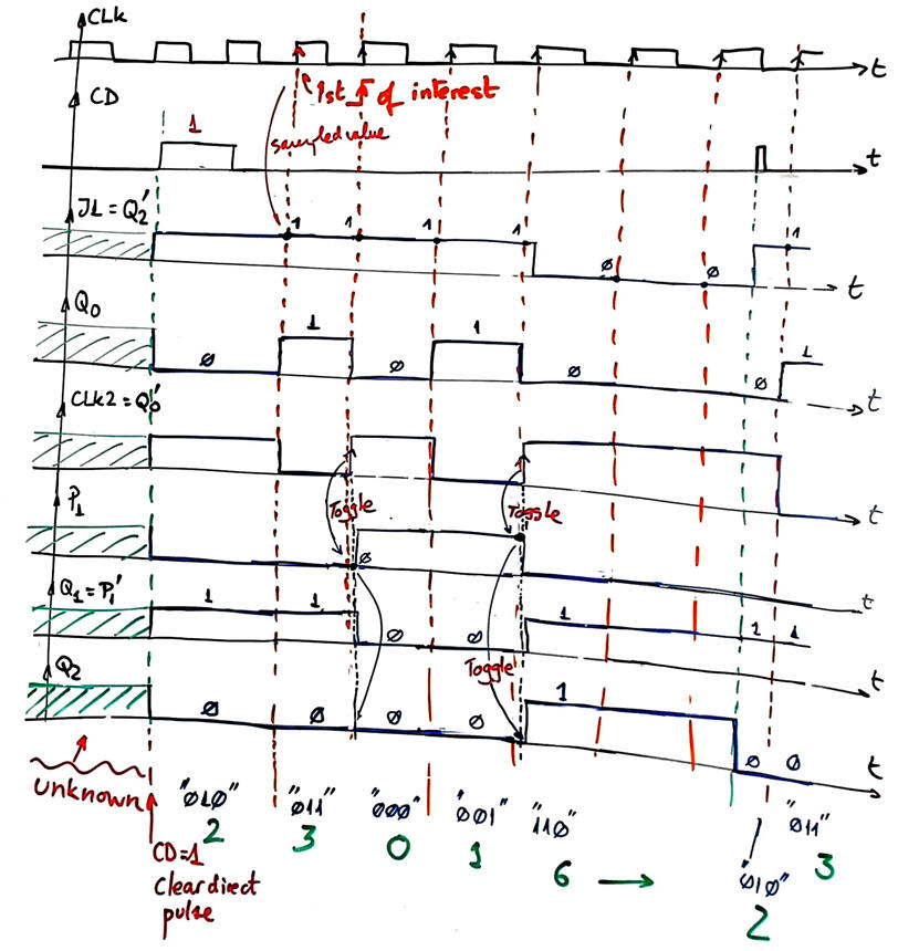
Fig 4. Typical CLK and CD waveforms template on a sheet of paper. Vertical dotted lines will be placed on CLK rising edges of interest. |
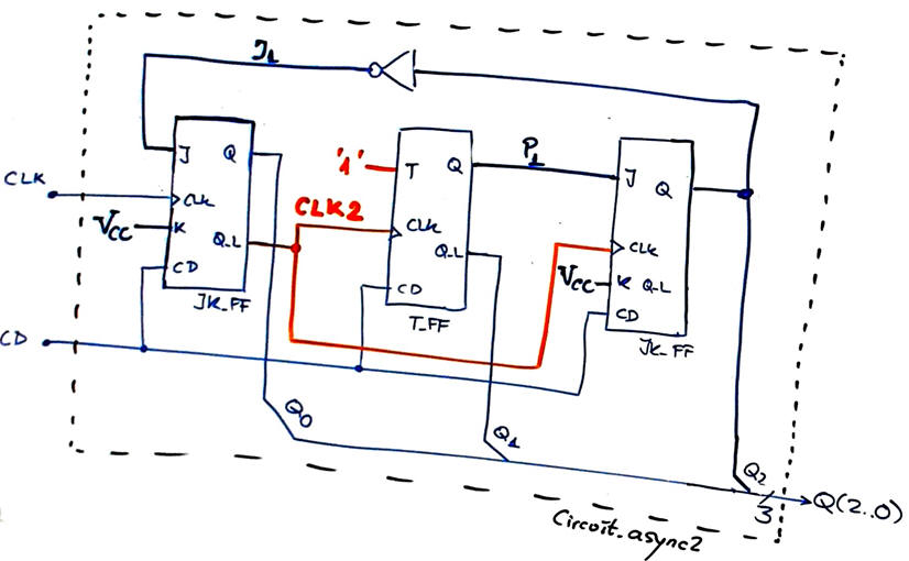
This circuit contains two CLK signals. It is asynchronous, because rising edges are not going to happen exactly at the same time, thus complicating the analysis.
Step #3: The complete circuit. Be sure to identify what T (or D, JK, RS) input values are sampled at the CLK's rising edge. To do it, consider the small tCO (in the range of ns) associated with each output transition. Add text discussing what is happening after each active CLK edge.
| Specifications | Planning | 3. Developing | Testing | Report |
Step #1: Study one FF driving inputs with CLK and signals.
Step #2: Solve a circuit with two CLK signals.
Step #3: Try now to analyse the complete circuit.
K and T inputs are always sampled '1'. J sampled values will depend on Q evolution.
| NOTE: Explain using arrows and graphic annotations what happens and when and how it works as time passes. Timing diagrams and solutions will not be considered valid without such explanations and discussions. |
 |
|
Fig. 5. Example of timing diagram and analysis discussion. |
Once the timing diagram is completed, determine the number of states and what is the binary output for each state. This circuit is capable of memorising 5 states: 2 - 3 - 0 - 1 - 6
Discuss what may be the function or the circuit's application, if any. It seems that it does not have a clear application unless it is to generate a five-number pattern at the CLK's speed.
What is the circuit's main problem? Why is this design a bad idea for precision applications? In P6 we can design better circuits using canonical synchronous FSM to generate this pattern of numbers.
| Specifications | Planning | Developing | 4. Testing | Report |
Testing means checking or verifying that the solution is correct and agrees with the initial specifications.
In this analysis section, the simplest way to check the timing diagram is by comparison with solutions from other methods.
| Specifications | Planning | Developing | Testing | 5. Report |
Project report: sheets of paper, scanned and annotated figures, file listings, notes or any other resources. In CSD, follow this rubric of indications for writing reports.
| Top | Method I | Circuit_async2 method II | Method III |
| 1. Specifications | Planning | Developing | Testing | Report |
Analyse Circuit_async2 as represented in Fig. 1 based on flip-flops using method II capturing the circuit in Proteus and running simulations using the logic analyser instrument. Answer these questions:
- Obtain the timing diagram.
- Determine what kind of output codes Q(2..0) are generated in each CLK cycle.
- What is the function of this circuit?
- Measure propagation delays CLK to output (tCO) and deduce the maximum CLK frequency, fCLK_max, that can be applied to the circuit.
|
|
Fig. 1. Symbol and schematic of the asynchronous circuit to be analysed. CLK is a rectangular wave of TCLK period. Clear direct (CD) is a single pulse any time the user likes to initialise the circuit. |
|
|
|
| Specifications | 2. Planning | Developing | Testing | Report |
Project location:
C:\CSD\P5\Circuit_async2\Proteus\(files)
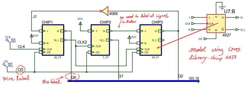
Choose Proteus as circuit simulator: draw/capture the circuit schematic in Proteus and run a simulation.
In CSD we never start a project or a simulation from scratch, but we copy and adapt from similar exercises found here on this digsys web.
Select a library of a classic technology, for instance LS-TTL or CMOS series 4000.
Use three steps:
- Step #1: Capture and run a circuit with only one FF
- Step #2: Add the second FF and run, check with the paper solution
- Step #3: Complete the full circuit and measure with the logic analyser.
| Specifications | Planning | 3. Developing | Testing | Report |
Draw your Circuit_async.pdsprj and simulate it in Proteus. Verify your solution using the logic analyser instrument. This is a Proteus circuit to play with flop-flops as if we were in the laboratory building such circuits for real using classic 4000 CMOS series. Use the procedure in several steps explained in the LAB5 note:
- Step #1: Capture and run a circuit with only one FF (for instance T_FF).
- Step #2: Add the second FF and run, check with the paper solution.
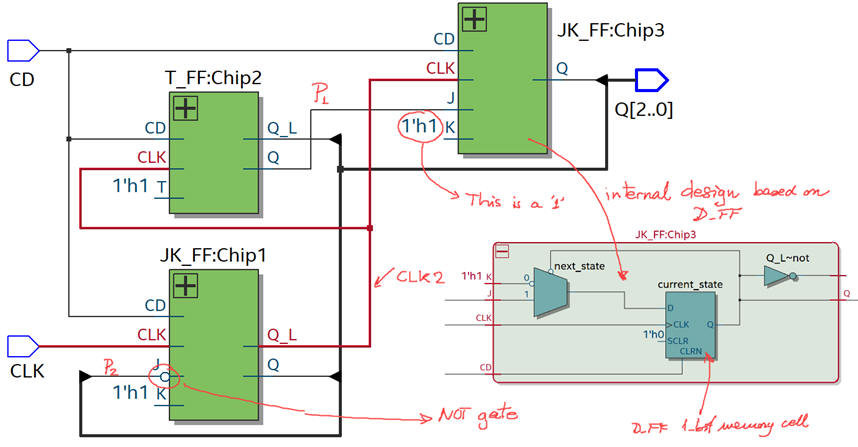
- Step #3: Complete the full circuit in Fig. 5. This is an example adaptation "Circuit_async2.pdsprj".
When picking parts from the library to mount your circuit, do this initialization --> Tool --> Global Annotator --> Total.
 |
|
Fig. 2. Example of circuit captured in Proteus. |
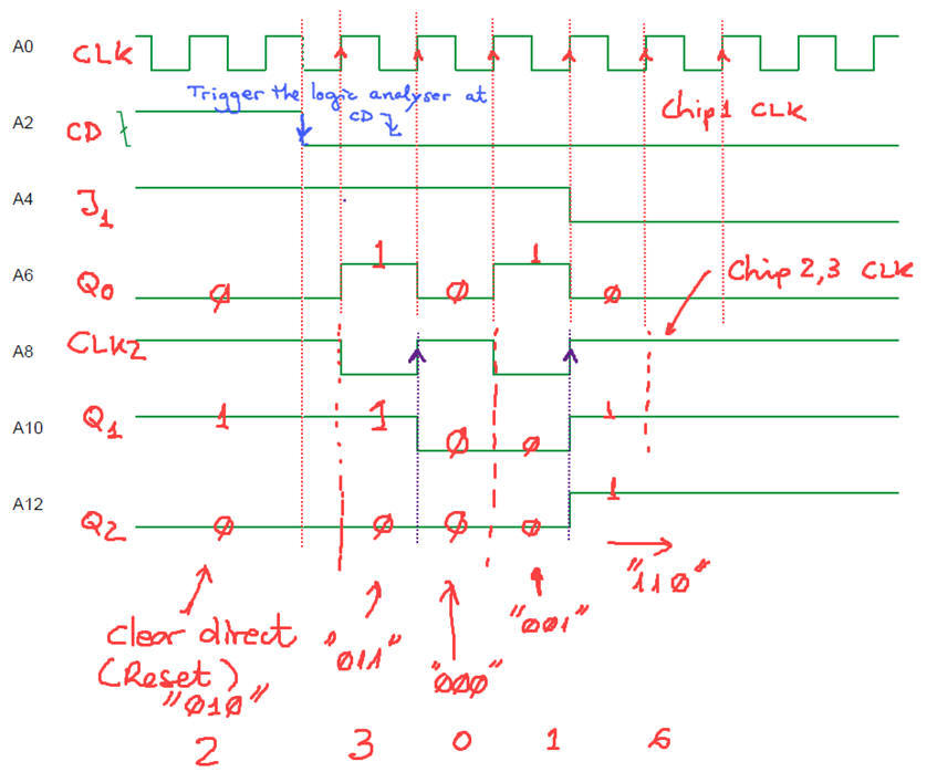
You can discuss logic analyser results from screen captures or, when reporting, from printed versions of the diagrams as shown in Fig. 3a.
 |
|
Fig. 3a. Example of circuit waveforms from the logic analyser printing. |
Thus, this circuit does not generate periodic signals, but a single event sequence with numbers: "2 --> 3 --> 0 --> 1 --> 6" after CD pulse.
Measuring propagation delays in Proteus simulations is possible by adjusting the time resolution of the logic analyser and the capture trigger (Fig. 3b). However, we can do it much better using ModelSim gate-level simulations applying the next analysis method.
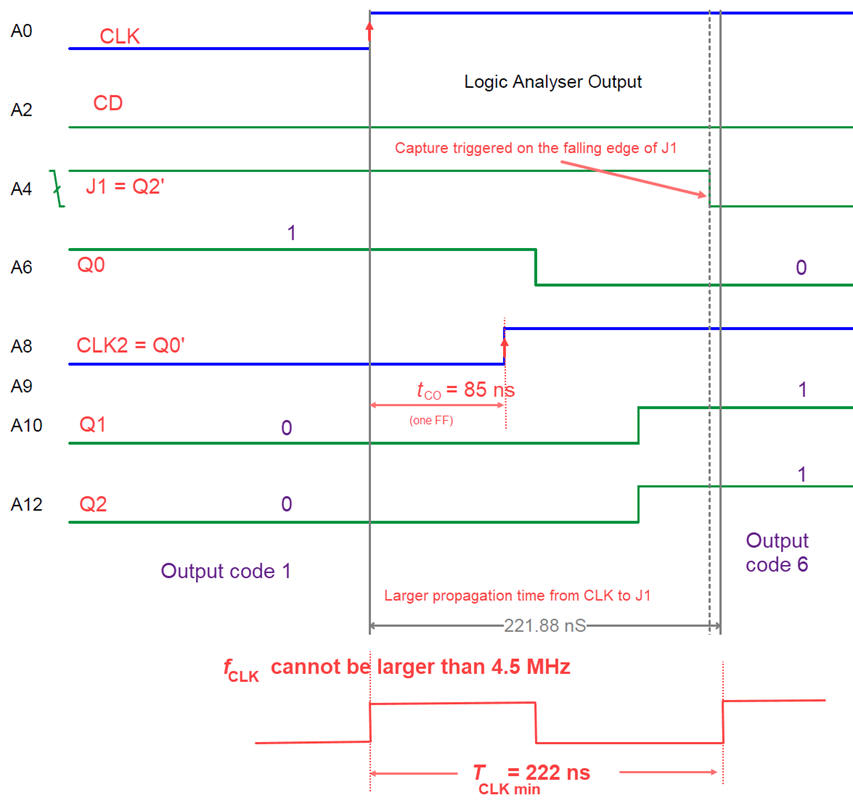 |
| Fig. 3b. Using the Proteus logic analyser to zoom signals in a given transition, from code 1 to code 6. The longest propagation delay is tP = 222 ns. Asynchronous circuits where the CLK is chained are slower than synchronous circuits where there is only one CLK driving all FF. |
| Specifications | Planning | Developing | 4. Testing | Report |
Testing involves verifying that the solution is correct and aligns with the initial specifications.
In this analysis section, the simplest way to validate the timing diagram is by comparing it with solutions from other methods.
| Specifications | Planning | Developing | Testing | 5. Report |
Project report: sheets of paper, scanned and annotated figures, file listings, notes, or any other resources. In CSD, follow this rubric of indications for writing reports.
| Top | Method I | Method II | Circuit_C Method III |
| 1. Specifications | Planning | Developing | Testing | Report |
Analyse Circuit_async2 represented in Fig. 1 based on flip-flops using method III: capture the circuit in VHDL as a plan C2 structure. Synthesise the project. Perform functional simulations based on a testbench to obtain timing diagrams. Discuss the drawbacks associated with asynchronous designs running gate-level simulations. Pay attention to the outputs zooming around CLK transitions and explain what happens from one output code to the next.
Answer these questions:
- Obtain the timing diagram.
- Determine what kind of output codes Q(2..0) are generated in each CLK cycle.
- What is the function of this circuit?
- Measure propagation delays CLK to output (tCO) and deduce the maximum CLK frequency fCLK_max that can be applied to the circuit.
|
|
Fig. 1. Symbol and schematic of the asynchronous circuit to be analysed. CLK is a rectangular wave with a TCLK period. The Clear Direct (CD) signal is a single pulse that can be activated by the user to initialise the circuit at any desired time. |
|
|
|
| Specifications | 2. Planning | Developing | Testing | Report |
Project location:
C:\CSD\P5\Circuit_async2\VHDL\(files)
Redraw the circuit proposed in Fig. 1 and fully annotate it as in Fig. 2 before translating and developing the VHDL project. This is a plan C2 project that consist of three files.
 |
|
Fig. 2. Circuit fully annotated and ready for translation to VHDL. |
Choose a target FPGA. Synthesise the circuit and simulate.
| Specifications | Planning | 3. Developing | Testing | Report |
Translate the Fig 2 schematic into VHDL (Circuit_async.vhd). The toggle flip-flop description in VHDL is available in its tutorial T_FF. The JK flip-flop description is available in JK_FF.
Synthesise the project Circuit_Async2_prj for a MAXII EPM2210F324C3 chip (later on, you can change the target chip to a Cyclone IV EP4CE115F29C7 device and compare performances).
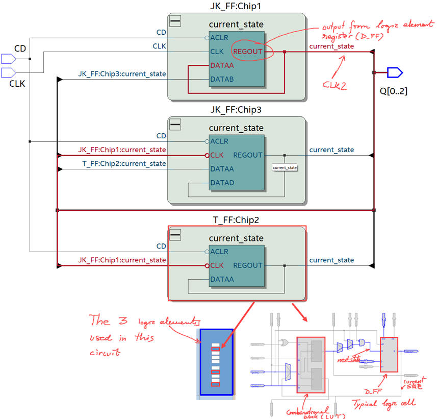
Inspect and analyse the RTL schematic generated by the synthesiser EDA tool as shown in Fig 3.
 |
|
Fig. 3. RTL produced by the synthesiser. |
Inspect and analyse the technology schematic generated by the synthesiser EDA tool as shown in Fig 4. How many registers (D_FF) are used?
 |
|
Fig. 4. Technology schematic to be tested using gate-level simulations. |
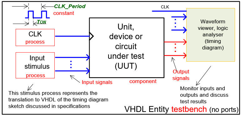
Fig. 5 shows the generalised VHDL testbench schematic that we have in mind to run simulations for our sequential systems under test. Note the significant change replacing Chapter 1 Min_Pulse constant by this new Chapter 2 CLK_Period to define the time resolution from now on. Any event shorter than a CLK period is not "seen" by the digital system.
 |
|
Fig. 5. General testbench fixture for sequential systems, including at least two stimulus processes: one for the CLK and another for the remaining input ports. |
Fig. 6 represents the inputs required in this experiment. A periodic CLK waveform of rectangular shape, for instance with a duty cycle = 25% and a clear direct CD pulse that can be repeated when necessary to initialise again the circuit. Make all the timing relative to the constant CLK_Period, that is the equivalent in Chapter 2 to the Chapter 1 constant Min_Pulse.
 |
|
Fig. 6. CLK and CD activity to be described in the testbench processes. From this activity the simulator will calculate outputs. Normal operation of the circuit can be inspected for example setting CLK_Period = 4 us. And detailed time measurements on signal transitions can be performed setting CLK_Period = 40 ns when testing the real technology view synthesised circuit for a given target chip (FPGA or CPLD). |
Start the testbench template and add CLK and inputs activity translating input signals in the timing diagram. Thus, to test sequential systems at least two stimulus processes will be required: the CLK process and another process for all the other inputs. This is an example testbench file Circuit_async_tb.vhd.
Functional simulation. Run the EDA VHDL tool and demonstrate how the circuit works adding comments to the printed sheet of paper containing the waveforms.
 |
|
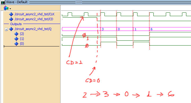
Fig. 7. Waveforms from functional simulation. This circuit looks like that is acting as a 4-bit binary counter in radix-2. |
Gate-level simulation. Run the EDA VHDL tool using the same test bench and demonstrate CLK to output propagation delays (tCO) and calculate the maximum frequency of operation.
|
Fig.8. Results from a gate-level simulation zooming all the test time to see that it works as expected. |
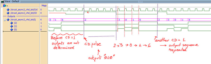
And in Fig. 9 below you see the signals in a given transition.
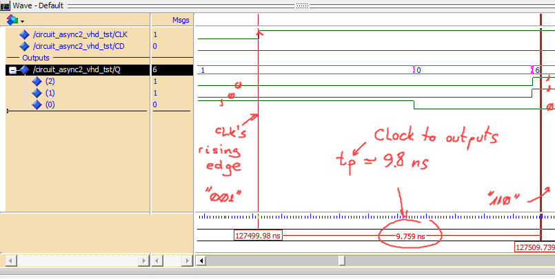 |
|
Fig. 9. Results from a gate-level simulation focusing a single transition in ns time resolution window. |
How about the timing analyser tool? Is is easy to use and obtain results in such circuits with several CLK signals?
| Specifications | Planning | Developing | 4. Testing | Report |
Testing means to check or verify that the solution is correct and agrees with the initial specifications.
In this analysis section, the simplest way to check the timing diagram is by comparison with solutions from other methods.
| Specifications | Planning | Developing | Testing | 5. Report |
Project report: sheets of paper, scanned and annotated figures, file listings, notes or any other resources. In CSD follow this rubric of indications for writing reports.
6. Prototyping
Use training boards and perform laboratory measurements to verify how the circuit works.
|
|
What goes next?
- Thus, in the end, if these asynchronous circuits behave so poorly, what is the right way to design reliable sequential circuits? The answer in next P6: Synchronous canonical sequential circuits based on FSM architecture.
| Home Term 26/27-Q1 Contact Products Electronic devices and companies Software Books Magazines Instruments DEE Library EETAC DEEL |

|
|
| Web activa des de 09/2001, @ F. J. Robert, Web editat amb Microsoft Expression Web 4. El contingut és un complement als materials d'estudi del curs Circuits i Sistemes Digitals disponibles al campus digital Atenea. Llicència:Reconeixement 4.0 Internacional de Creative Commons |