|
|
Bachelor's Degree in Telecommunications Systems and in Network Engineering |
|
|
|
||
|
|
Using and designing JK flip flop (JK_FF) |
|
|
|
||
1. Specifications
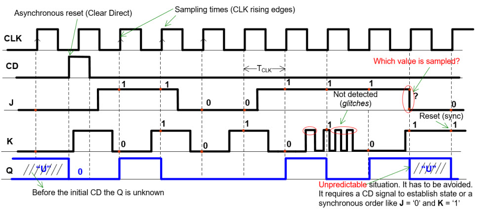
A. Design a synchronous 1-bit memory cell type JK flip-flop (JK_FF) using the FSM strategy. It can be used to store/save/write/register a 1-bit of information, as a frequency divider by 2 or as the basic block to implement digital counters and data registers. As you see in the chip's function table represented in Fig. 1, at the CLK's rising edge, the next output value (Q+) will depend on the logic values sampled at the inputs J and K and also on the current stored internal state (Q).
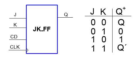 |
Fig. 1. Symbol, function table and example timing diagram of a JK flip-flop. Clear direct (CD) is the asynchronous reset. Be aware on how the J and K inputs has to be stable before the sampling edge, because if not, the output is unpredictable. (Visio). Commercial classic JF_FF chips: CMOS HEF4027B; TTL-LS SN74LS73A |
 |
|
B. Perform a gate-level simulation of the circuit to measure its CLK to output time (tCO) and thus, the maximum frequency of operation for a target chip manufactured using a given technology.
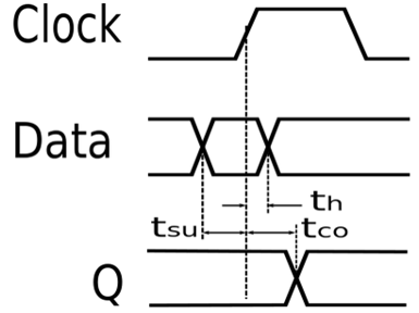 |
Fig. 2. Flip-flop setup (tSU), hold (tH) and clock to output (tCO) timing parameters (ref.) For a given technology, tCO determines the minimum CLK period, as the outputs must be stabilised before applying another CLK rising edge. See more details in this L5.3 lecture. |
2. Planning
As always, the aim of the planning section is to obtain a schematic or flow chart that can be automatically translated to VHDL.
First of all, let's study the basics of the 1-bit memory devices (asynchronous latches and synchronous flip-flops). How are they designed? How do they work? Now, it is right continuing with the design of a D_FF so that you get an idea of what is the CLK and how it works.
And, once the theory understood, let us apply the FSMmethodology to build and test the JK_FF as a single file project. This procedure with slight variations is going to be repeated in all the FSM projects.
1) Figure out the state diagram. Number of states and conditions of transitions. Write the outputs at each state in parenthesis and using another colour.
2) Particularise the general FSM topology in Fig. 3 to this problem and answer these questions:
a) State register based on D_FF. Number of bits for the current and next state coding (r). [ r = number of states if one-hot; r = (1/log 2)·log (number of states) if binary or Gray]. How many 1-bit registers (D_FF) will the circuit contain?
b) To which block is connected every input and output port?
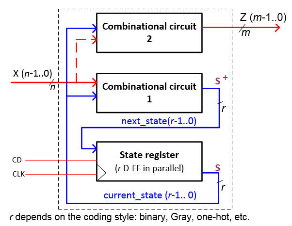 |
Fig. 3. Topology and description of the FSM used in CSD. (Visio). |
3) Draw the state register. We'll use always the same VHDL code description.
4) Output logic (CC2), required to calculate the outputs at each state. Truth table, and flow chart if a behavioural description is used, which is normally the best idea because in this way the Boolean algebra is left to the synthesiser.
5) Next state logic (CC1), required to calculate the next state to go after the CLK's rising edge. Truth table, and flow chart using a behavioural description, which is normally the best idea because the equations are left to the synthesiser.
6) Project folder location and file name (JK_FF.vhd):
<disk>/CSD/P5/JK_FF/(files)
3. Development
Write down the VHDL file corresponding the JK_FF after having translated the flow charts of the CC1 and CC2 and copied the state register. Copy and adapt a previous example, for instance the T_FF.
The name of the source file is JK_FF.vhd. Run the EDA tool to synthesise the circuit and print and comment the RTL schematic. Check the number of registers (D_FF) used in the target chip. In this simple example, the answer has to be a single D_FF register.
This basic flip-flop can be used as well as a component in other designs where a 1-bit memory cell would be required.
NOTE: This translation JK_FF.vhd is the implementation of the JK_FF that also includes an asynchronous set direct (SD) input. You can use it in P5 method 3 analysis when the application circuit contains JK_FF (or RS_FF) components that require both asynchronous signals CD and SD.
Asynchronous set direct (SD) is implemented in classic chips such 4027B. However, some FPGA cells do not include registers (D_FF) with SD input, and so, if required it has to be implemented using extra logic elements. For instance MAX II includes an asynchronous load that can be used as SD, but MAX10 and Cyclone IV devices have to implement SD using external additional logic elements.
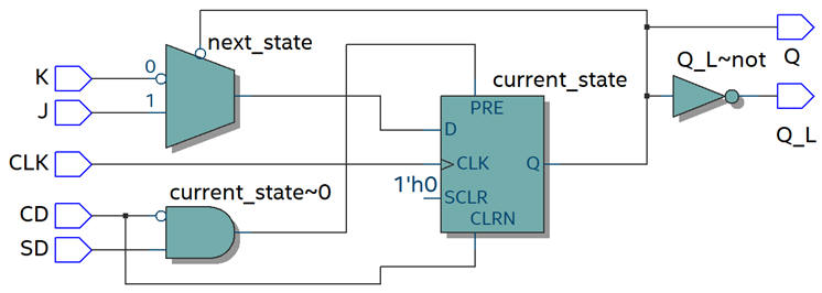 |
| Fig. 4. a) RTL circuit for the JF_FF that includes SD (CD has precedence over SD). |
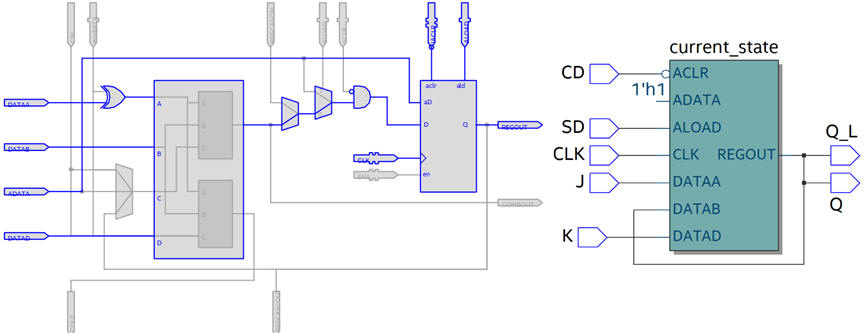 |
| Fig. 4. b) Logic element of a MAXII implementing a JK_FF with SD. To implement the SD, the logic cell contains a D_FF that includes an asynchronous load (ALOAD) that loads ADATA = '1'. |
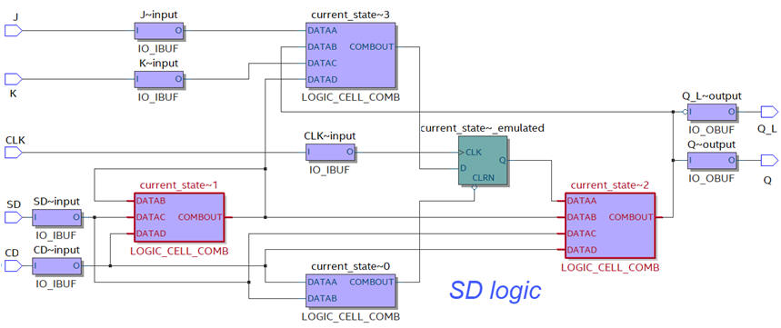  |
| Fig. 4. c) Implementation of the JK_FF with SD in a MAX10. Several combinational circuits are required to implement the asynchronous SD because the D_FF register does not include such input. |
4. Testing (functional simulation)
This in Fig. 5 is the VHDL testbench schematic that we have in mind to run simulations. To test CLK-driven sequential systems at least two concurrent stimulus processes will be required: one process for the CLK and another one for all the other input signals.
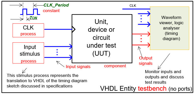 |
| Fig. 5. Testbench where to make it easy the CLK is another concurrent process. (visio) |
For testing the circuit JK_FF the general schematic in Fig. 5 is adapted as shown in Fig. 6.
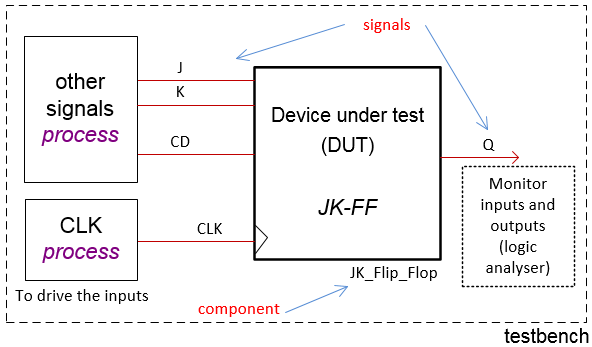 |
Fig. 6. VHDL testbench. Let's use different processes to drive the inputs and the CLK. |
Start the test bench template and add the CLK and inputs activity translating the timing diagram in Fig.1. Make all the timing relative to the CLK_Period constant, which is the equivalent in Chapter 2 to the Chapter 1 constant Min_Pulse.
This JK_FF_tb.vhd is an example of test bench file (use only constant and stimulus processes).
Functional simulation. Run the EDA VHDL tool and demonstrate how the circuit works adding comments to the printed sheet of paper containing the waveforms.
NOTE: this JK_FF_tb.vhd is an example of test bench file (use only constant and stimulus processes) for a JK_FF that has both CD and SD initialisation signals.
5. Testing (gate-level and timing analyser)
Gate-level simulation. Run the EDA VHDL tool using the same test bench and measure the CLK to output propagation time(tCO) and the maximum frequency of operation for a given CPLD or FPGA target chip.
Run the EDA tool timing analyser to check results.
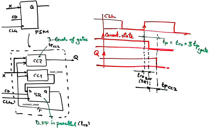
The idea behind calculating the maximum speed of operation is the same for all FSM conceived using the proposed architecture in Fig. 3. Even if for a simple flip-flop CC2 contains less than 3-levels-of-gates, it still will be a good approximation. The real propagation delay will depend on the FPGA or CPLD technology and final assembled circuit by the synthesis tools.
6. Prototyping
Use training boards and perform laboratory measurements to verify how the circuit works.
7. Report
It is required a handwritten original project report containing sections 1 - 2 - 3 - 4 - 5, scanned figures with annotations, file listings, diagrams, sketches or any other resources. Theory stuff to comprehend how the circuit works may be included in section 1 on specifications.
| Home Term 26/27-Q1 Contact Products Electronic devices and companies Software Books Magazines Instruments DEE Library EETAC DEEL |

|
|
| Web activa des de 09/2001, @ F. J. Robert, Web editat amb Microsoft Expression Web 4. El contingut és un complement als materials d'estudi del curs Circuits i Sistemes Digitals disponibles al campus digital Atenea. Llicència:Reconeixement 4.0 Internacional de Creative Commons |