|
|
Bachelor's Degree in Telecommunications Systems and in Network Engineering |
|
Chapter 1 problems |
- D1.13 - |
3-digit BCD subtraction using Subt_1bit |
1. Specifications
Page to be updated because a more convenient name for this project is Subt_BCD_3digit. Modify the number range to 999.
We want to implement a circuit for subtracting 8-bit binary radix-2 numbers as represented in Fig. 1. Including additional circuits we can input operands directly in BCD and represent results in 7-segment displays, which are quite convenient features. In this way we can use the project for learning many Chapter 1 concepts on logic and arithmetic blocks.
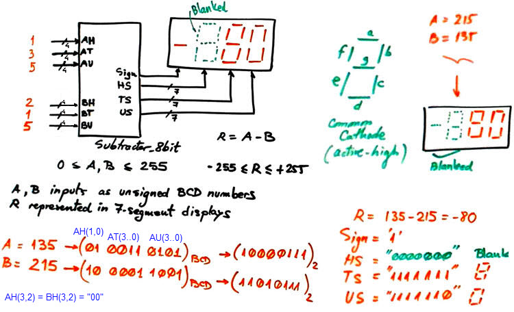 |
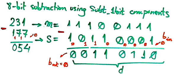
Fig. 1. The entity of a Subtractor_8bit and an example operation. Internal circuits will subtract in binary radix-2. |
In chapter 2 we can easily introduce a keyboard and data registers to save or register operand numbers before calculating results, as in typical calculators. The same project B3.13 is proposed in Chapter 3 for learning the basics of μC software organisation and basic digital I/O.
In this project, for academic purposes, as a variation to the typical arithmetic circuits proposed in P4 for working with integer numbers, we will implement substation operations using true subtractors and introducing a correction mechanism for representing negative numbers in 7-segment displays.
Draw some values of the circuit's truth table as in Fig. 2. You can try more operands.
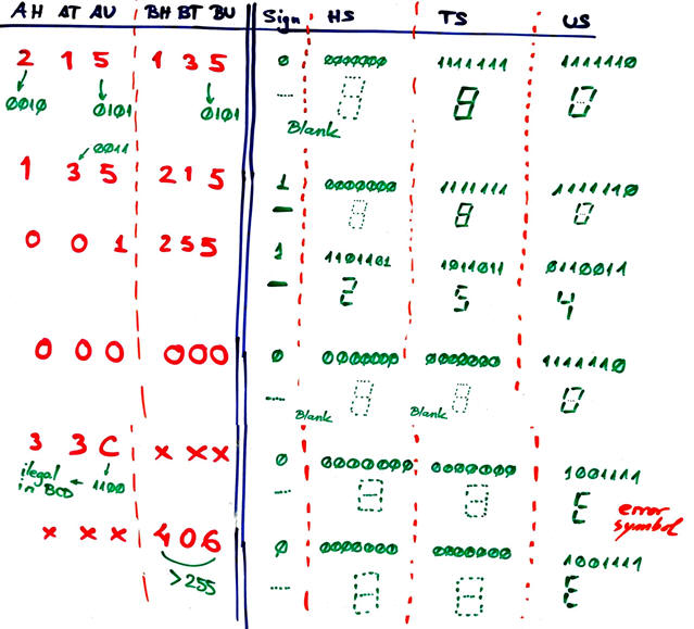 |
Fig. 2. Subtractor_8bit example truth table values. |
Draw an example of timing diagram to be used later as stimulus in the VHDL verification of the synthesised circuit. You can use as example test vectors for operands A (minuend) and B (subtrahend). Add other numbers if you liked it.
-
Option #1: Min_Pulse = 3.7 ms. Values for subtrahends and minuends: 214, 133, 12, 0, 255, 101, 2A6, 578
-
Option #2: Min_Pulse = 103 ms. Values for subtrahends and minuends: 231, 18, 121, 0, 111, 255, B03, 678
-
Option #3: Min_Pulse = 5.3 ms. Values for subtrahends and minuends: 31, 189, 199, 0, 254, 3, 03F, 833
|
|
Fig. 3. Timing diagram example for the Subtactor_8bit considering for the test vectors. |

2. Planning
The hierarchical architecture proposed for solving this project is represented in Fig. 4. To obtain a variety of solutions we also include options for the components to allow us covering much of the Chapter 1 content.
|
|
Fig. 4. Proposed fully-annotated architecture for the full Subtractor_8bit ready for VHDL translation. |
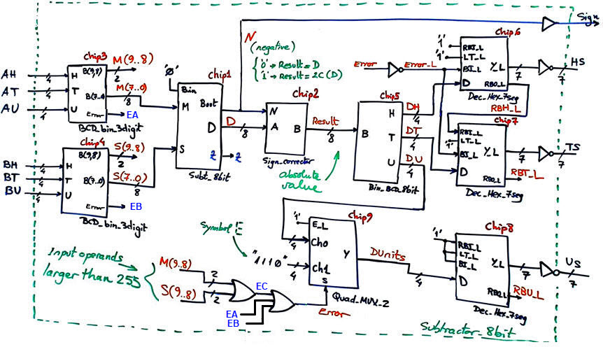
As shown, Chip 3 and Chip4 convert the input BCD numbers A and B to binary radix-2 M and S. They also generate EA and EB, error signals to be high when any BCD input is larger than '9'. And using gates and the most significant bits of M and S, we can also detect using EC when input numbers are larger than '255', overflowing the range of Chip1 to perform subtractions. This Error signal is connected to Chip6, Chip7 and Chip9 to be able to blank the 7-segment displays HS and TS while showing in US the symbol 'E'.
Let us identify the several projects included in this design.
Project 1 is the main top design in Fig. 4. Project location:
C:\CSD\PLA2_3\Subtractor_8bit\(files)
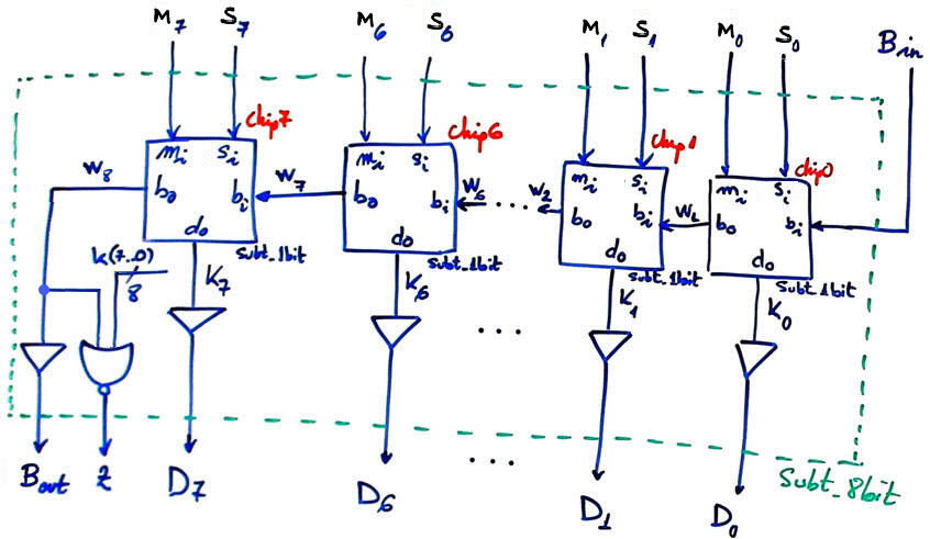
Project 2 (Chip1 in Fig. 4) is the Subt_8bit represented in Fig. 5. It shows how to chain Subt_1bit using plan C2 to generate true subtractors of any size, for example, the Subt_8bit required in this project. It looks quite similar to what was proposed for chaining standard adders.
Hence, for building a Subt_nbit we chain up to n Subt_1bit components by rippling borrow signals in the same way we connect carries when building our ripple-carry adders in LAB3.
The strategy to design the key component Subt_8bit is to use plan C2 chaining up to eight 1-bit subtractors Subt_1bit instead of the standard way based on 1-bit adders and two's complement convention discussed in P4.
|
|
Fig. 5. The internal architecture for our Subt_8bit chaining Subt_1bit components. |
This device will work correctly only for natural numbers where M > S. Thus, deduce which kind of algorithm and circuits may be used to display correct values even for negative results (this will be the task for Chip 2 in Fig. 4).
|
|
Fig. 6. Example operation when using the Subt_8bit for A < B. Perform other similar operations to visualise the algorithm required for correcting negative results and being able to display them correctly. |

Project location:
C:\CSD\PLA2_3\Subt_8bit\(files)
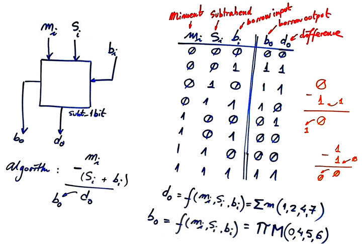
Project 3 is the Subt_1bit represented in Fig. 7 along with its truth table, which is the component repeated up to eight times in Fig. 5.
|
|
Fig. 7. The idea of the basic Subt_1bit and its truth table. This basic circuit has three inputs (minuend, subtrahend and borrow) and two outputs (difference and borrow), similarly to the basic Adder_1bit. |
We can practice using several CSD design strategies presented in L1.4.
Option #A.1: plan A. Equations using only NAND2 gates.
Option #A.2: plan A. Equations using Subt_1bit using PoS.
Option #B.1: plan B. Truth table captured using a schematic.
Option #B.2: plan B. Truth table captured using a flowchart.
Option #C2.1: plan C2. Using the MoD
Option #C2.2: plan C2. Using the MoM and MUX_2
Project location:
C:\CSD\PLA2_3\Subt_1bit\(files)
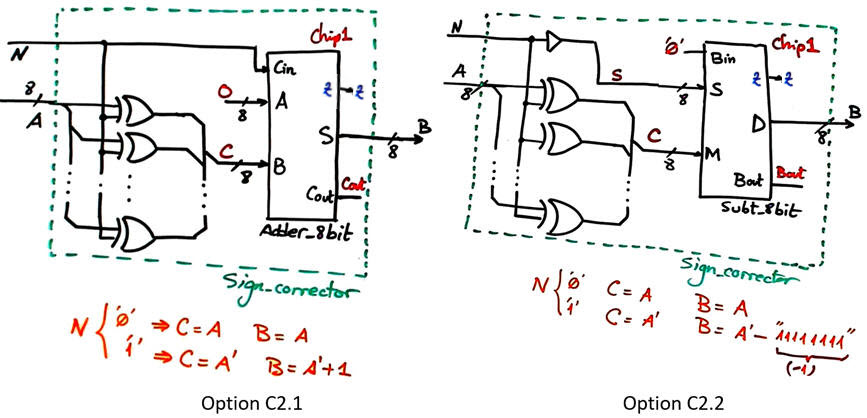
Project 4 is the Chip2 Sign_corrector in Fig. 4.
When the result from Chip1 generates Bout = '1' = N the numbers to represent on the displays will be negative. We need to represent the result's absolute value accompanied by the sign LED. This is the task for this Chip2 and this correction algorithm is explained in Fig. 8.
|
|
Fig. 8. Example operations to generate the absolute value with the Sign_corrector. |
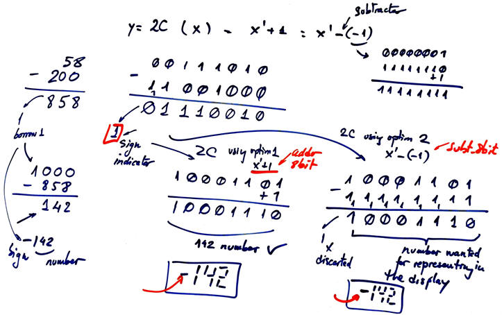
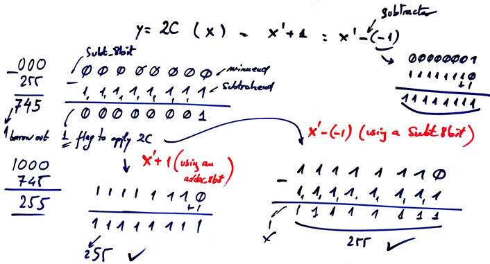
This Sign_corrector can be designed internally using two options as shown in Fig. 9. The idea is to calculate the two's complement when N = '1' and do nothing when N = '0' (buffer). The two's complement can be obtained using both Adder_8bit as presented in P4 and also using another Subt_8bit like the one presented in Fig. 5.
Options for this project:
Option #C2.1: plan C2. Using an Adder_8bit
Option #C2.2: plan C2. Using the Subt_8bit
|
|
Fig. 9. Two schematics for implementing the Sign_corrector. |
Project location:
C:\CSD\PLA2_3\Sign_corrector\(files)
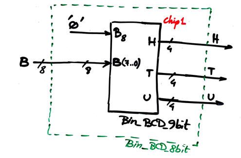
Project 5 is the Chip5 in Fig. 4, the code converter Bin_BCD_8bit solved applying plan C2 from our similar products, for instance in Bin_BCD_9bit. Any input from 0 to 255 in radix-2 will be translated to BCD as the three digits hundreds, tens and units.
|
|
Fig. 10. This is how to use a Bin_BCD_9bit as the Bin_BCD_8bit required in this application. |
We propose two alternatives for the basic component DM74185 included in the circuit:
Option #A: plan A. Equations from Minilog
Option #B: plan B. Truth table or algorithm captured using a schematic or flowchart
Project location:
C:\CSD\PLA2_3\Bin_BCD_8bit\(files)
Project 6 is Chip3 and Chip4 in Fig. 4, the code converter BCD_bin_3digit solved applying plan C2 from our similar products.
We simply use the conversion chain based on DM74184 components proposed in D1.15 to obtain the output B. representing the binary radix- 2 number.
As shown in Fig. 4, these chips also generate the Error signals to be high when any BCD input is larger than '9'. To generate such flag output we can use for instance three Comp_4bit and logic gates, as shown in Fig. 10. Complete and draw the full circuit in single sheet before translating it to VHDL.
|
|
Fig. 11. Error signal implementation to detect when any of the three BCD inputs is larger than '9'. |
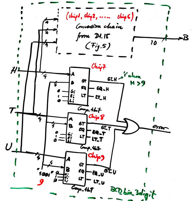
In our product section you can find the Comp_4bit solved as plan A or the same Comp_4bit solved using plan C2.
Project location:
C:\CSD\PLA2_3\BCD_bin_3digit\(files)
Project 7 are the Chip1, ... Chip 6 in Fig. 11, the DM74184. And we can imagine to options:
Option #A: plan A. Equations from Minilog
Option #B: plan B. Truth table or algorithm captured using a schematic or flowchart
Project location:
C:\CSD\PLA2_3\DM74184\(files)
Project 8 are the Chip6, Chip7, Chip8 in Fig. 4: decoders hexadecimal to 7-segments Dec_Hex_7seg using one of the two options for its internal component Hex_7seg_decoder:
Option #A: plan A. Equations from Minilog
Option #B: plan B. Truth table or algorithm captured using a schematic or flowchart
Project location:
C:\CSD\PLA2_3\Dec_Hex_7seg\(files)
Project 9 is the Chip9 in Fig. 4: quadruple 2-channel multiplexer (Quad_MUX_2) using one of these two options:
Option #B: plan B. Truth table or algorithm captured using a schematic or flowchart.
Option #C2: plan C2. Using MUX_2 components and other logic if necessary (circuit expansion)
Project location:
C:\CSD\PLA2_3\Quad_MUX_2\(files)
3. Developing
Develop the circuit targeting the board DE10_Lite chip MAX 10. Work bottom-up, completing one project at a time.
4. Testing (functional)
Test your circuit writing a VHDL simulation testbench from the timing diagram in the specifications (Fig. 3). As we usually do, start drawing your testbench fixture diagram.
Work bottom-up, testing one project at a time.
5. Testing (gate-level)
Indications for PLA4. Test your circuit and measure both, propagation delays in a given transition and the Subtractor_8bit theoretical maximum operational speed (millions of operations per second).
New project location to continue with section #5 (copy your circuit and testbench vhd files and start a new project):
C:\CSD\PLA4\Subtractor_8bit\(files)
CPLD or FPGA target chip options to compare and discuss results:
Target option #1.: MAX II
Target option #2.: Cyclone IV
(*) MAX10 chips are not used because Intel Quartus does not generate the "*.sdo" file for running gate-level simulations.
Annexes
Explain and report the full design 1 - 2 - 3 - 4 of the components that you invent and that are not found in our libraries.
In a single sheet, describe the symbol and truth table of the components used already available in CSD products.
Lab groups and teamwork
Start studying the top circuit and how it may work. Imagine its internal architecture counting the number of projects involved and the total numbers of VHDL files that will be required, whatever you are inventing them or copying directly from other CSD products.
Options for designing some of the components in the chips. Study individually each project specifications in detail. Large circuits are all of them plan C2, and its architecture is proposed or can be found or adapted from CSD products.
|
Project 3 Subt_1bit |
Project 4 Sign_corrector |
Project 7 DM74184 |
Project 5 DM74185 |
Project 8 Hex_7seg_decoder |
Project 9 Quad_MUX_2 |
Operands for timing diagrams and test benches | |
| Group 1 | A.1 | C2.1 | A | B | A | C2 | 1 |
| Group 2 | A.2 | C2.2 | B | A | B | B | 2 |
| Group 3 | B.1 | C2.1 | A | B | A | C2 | 3 |
| Group 4 | B.2 | C2.2 | B | A | B | B | 1 |
| Group 5 | A.2 | C2.1 | A | B | A | C2 | 2 |
| Group 6 | C2.1 | C2.2 | B | A | B | B | 3 |
| Group 7 | C2.2 | C2.1 | A | B | A | C2 | 1 |
Follow this rubric for writing reports. Because two complete projects are solved, this assignment will be is at least eight sheets of paper long report.
| NOTE: This post-lab assignment must be solved only after having completed successfully lab sessions LAB2 and LAB3 because you will adapt and apply materials and proceedings from them. |
| Home Term 26/27-Q1 Contact Products Electronic devices and companies Software Books Magazines Instruments DEE Library EETAC DEEL |

|
|
| Web activa des de 09/2001, @ F. J. Robert, Web editat amb Microsoft Expression Web 4. El contingut és un complement als materials d'estudi del curs Circuits i Sistemes Digitals disponibles al campus digital Atenea. Llicència:Reconeixement 4.0 Internacional de Creative Commons |