|
|
Bachelor's Degree in Telecommunications Systems and in Network Engineering |
|
Chapter 1 problems |
- D1.12 - |
16-bit comparator for 2C integer and radix-2 numbers |
1. Specifications
Build the comparator Sel_Int_Cmp_16bit represented in Fig. 1 for 16-bit two's complemented (2C) integer or radix-2 operands. For N = '1', the numbers are integers; for N = '0', the numbers are radix-2
The same project B3.12 (for 8-bit operands) is proposed in Chapter 3 for learning the basics of μC software organisation and basic digital I/O.
 |
| Fig. 1. Symbol. |
Specifications include: symbol, truth table, data range, example commercial chips with similar functionality, etc. You may like to add theory to better explain and comprehend these circuits.
Draw the testbench fixture and an example of timing diagram to be used later as stimulus in the VHDL verification of the synthesised circuit. Consider Min_Pulse = 53.6 ms. You can use as example test vectors for the integer operands A and B (add other numbers if you like):
-
Option #1: (+32760), (+18841), (-30504), (-22), (+18340), (-13740), 0, (+31220)
-
Option #2: (-31554), (+22780), (-19306), (+12408), (-5), 0, (-5545), (+15554)
-
Option #3: (-17306), (+30701), (+32767), (-29830), 0, (-13208), (+6), (-19301)
If we liked to test all the circuit, how long would it take to run the full verification?
Additional specifications for PLA4 for performing timing simulations and measurements:
Calculate the propagation delay in a given signal transition using gate-level simulations in VHDL.
Calculate the circuit's longest propagation delay and maximum speed for a given target chip using the timing analyser tool.
If we liked to test all the circuit, how long would it take?
Be aware that the location of this project enhanced with timing simulation and measurements (section 5) is:
C:\CSD\P4\Sel_Int_cmp_16bit\(files)
2. Planning
Invent the plan C2 schematic for this Sel_Int_Cmp_16bit after having studied the example Int_Comp_8bit and designing the Comp_16bit as indicated in the annex below.
We can start discussing the planning imagining the draft schematic in Fig. 2, as proposed for generic arithmetic and logic circuits in L4.2.
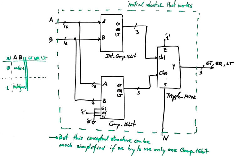 |
| Fig. 2. The general concept of comparisons with different data types. |
Now, after having studied in Int_Comp_8bit how integer comparisons are carried out using radix-2 comparators, we can draw the optimised and perfectly annotated schematic in Fig. 3 ready for VHDL translation.
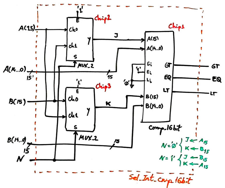 |
| Fig. 3. Schematic plan C2 ready for VHDL translation. |
Project location:
C:\CSD\P3\Sel_Int_cmp_16bit\(files)
3. Development
Circuit synthesis. Ideal RTL and technology views. CPLD or FPGA target chip options:
-
Option #1: MAX II EPM2210F324C3.
-
Option #2: MAX10 (*) 10M50DAF484C7
-
Option #2: Cyclone IV EP4CE115F29C7
(*) MAX10 chips are not used for running gate-level ModelSim simulation because Intel Quartus Prime does not generate the "*.sdo" file accompanying the "*.vho" translation of the technology view. Thus, you can run the timing analyser as usual, and change to another device family for performing examples of gate-level timing diagrams.
How many FPGA resources (logic cells, logic elements, etc.) are used? What is the percentage of the target chip used in this design?
4. Functional test
Testbench fixture and stimulus vectors.
4. Gate-level simulation and timing analysis
After having studied P4 tutorials, additional questions can be added to our report. For instance:
-
Perform a gate-level simulation to measure propagation delays in a given signal transition.
-
Deduce the worst-case propagation delay running the timing analyser tool and calculate the circuit's maximum frequency of operation for the target chip used in the design.
Annex: |
Comp_16bit |
16-bit comparator for radix-2 numbers |
Specifications
Build the 16-bit radix-2 comparator Comp_16bit represented in Fig. 1.
 |
| Fig. 1. Comp_16bit symbol. |
Specifications include: symbol, truth table, data range, example timing diagram and comparison operations, example commercial chip, etc.
Draw an example of timing diagram for the testbench fixture to be used later as stimulus in the VHDL verification of the synthesised circuit.
2. Planning
Two options are possible for this Comp_16bit:
-
Option #1: expanding Comp_4bit in a ripple chain plan C2. Draw and fully annotate your schematic to be ready for VHDL translation.
-
Option #2: Parallel tree expansion plan C2 as proposed in the architecture represented in Fig. 2.
 |
| Fig. 2. 16-bit tree comparator network adapted from this reference book: Ercegovac, M., Lang, T., Moreno, J. H., "Introduction to Digital Systems", John Wiley & Sons, 1999). It includes slides: Chapter 10 is on arithmetic circuits. This is Fig. 10.17 in the referenced book slides. |
Two options are possible for the component Comp_4bit:
-
Option #1: Using plan C2 to obtain a ripple comparator chaining expandable Comp_1bit as as shown in this project Comp_4bit.
-
Option #2: Using plan A equations as shown in this project Comp_4bit. This plan implies that the Comp_1bit component is not required.
And finally we got up to four proposals for inventing the Comp_1bit component, three of which are already available in our product examples:
-
Option #1: Comp_1bit plan A (minimised equations from the truth table in the form of PoS or SoP)
-
Option #2: Comp_1bit plan B (behavioural interpretation of the truth table)
-
Option #3: Comp_1bit plan C2 based on the method of multiplexers (MoM)
-
Option #4: Comp_1bit plan C2 based on the method of decoders (MoD) proposed as follows:
Find in our Comp_1bit tutorials the specifications (symbol, truth table, etc.). Study how the decoders work in L2.3, use the the Dec_4_16.vhd component to implement the Dec_5_32 required in this application following the ideas in Fig. 3.
 |
| Fig. 3. Designing a larger Dec_5_32 expanding Dec_4_16. |
| Home Term 26/27-Q1 Contact Products Electronic devices and companies Software Books Magazines Instruments DEE Library EETAC DEEL |

|
|
| Web activa des de 09/2001, @ F. J. Robert, Web editat amb Microsoft Expression Web 4. El contingut és un complement als materials d'estudi del curs Circuits i Sistemes Digitals disponibles al campus digital Atenea. Llicència:Reconeixement 4.0 Internacional de Creative Commons |