|
|
Bachelor's Degree in Telecommunications Systems and in Network Engineering |
|
|
|
||
|
|
Bin_BCD_9bit: plan C2 multiple VHDL files |
|
|
|
||
Structural design of a 9-bit binary radix-2 to BCD converter
1. Specifications
Design a 9-bit code converter from binary radix-2 to BCD using plan C2: hierarchical structure based on components of the same kind, for instance DM74185 and logic gates if necessary.
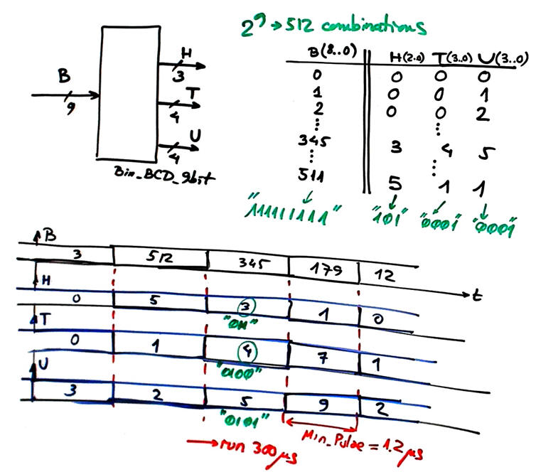
Bin_BCD_9bit has the symbol, truth table and example timing diagram represented in Fig. 1.
|
|
| Fig. 1. Symbol and truth table of the Bin_BCD_9bit chip. The truth table contain 2^9 = 512 combinations. |
This is the article from Wikipedia where to find information on how to organise the circuit structure: the double dabble algorithm is used to convert radix-2 numbers into BCD.
2. Planning
Structural hierarchical plan C2, a plan based on interconnecting or chaining components (circuit expansion) and extra logic when necessary. The idea comes from the commercial chip 74185A datasheet as shown in Fig.3, an optimised version of the double dabble algorithm that performs additions in parallel. This the component DM74185 implemented using plan B.
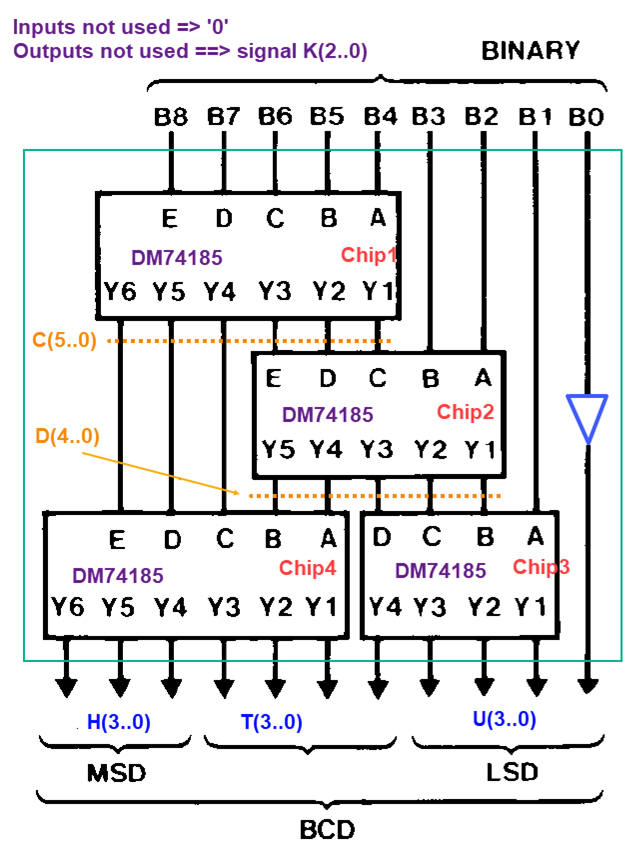 |
Fig. 3. Annotated schematic using the same picture from the 74185 datasheet. |
If Fig. 3 is not clear enough, it is better to draw it all again, annotating every component and signal. Thus the recoomended schematic ready for translation into VHDL is shown in Fig. 4.
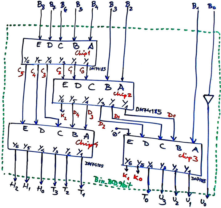 |
Fig. 4. Annotated schematic drawing all te circuit again. |
This is a two VHDL file project. Project location:
C:\CSD\P3\Bin_BCD_9bit\(files...)
3. Developing the project using EDA tools
Run a EDA project to synthesise the circuit. Select a target chip like Intel Cyclone IV EP4CE115F29C7.
VHDL translation of the top Bin_BCD_9bit.vhd in Fig. 4 above. Get the component from the DM74185 annex.
Fig. 5 shows an example of RTL schematic generated after the synthesis process.
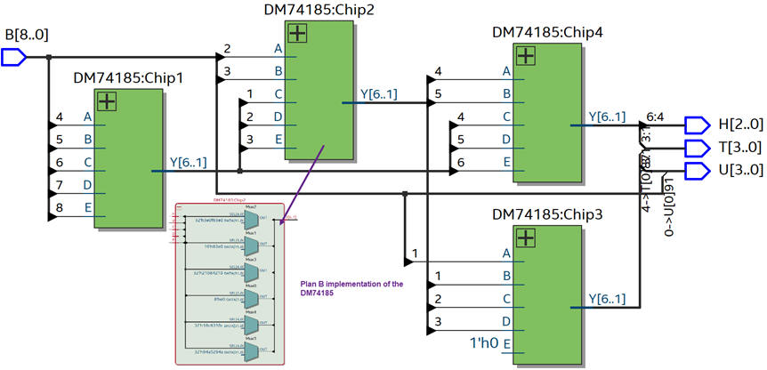 |
| Fig. 5. RTL view from Intel Quartus Prime. |
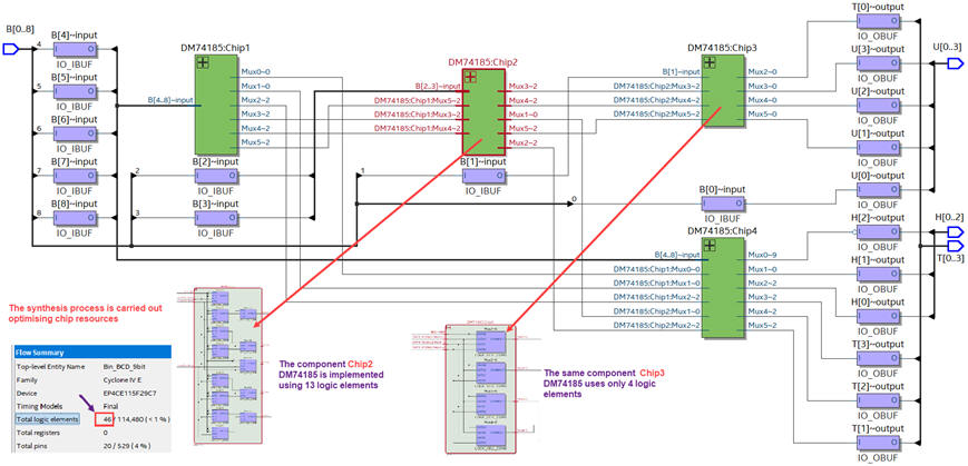
Fig. 6 shows how the circuit is synthesised using Cyclone IV logic resources.
 |
|
Fig. 6. Example technology view for a Cyclone IV FPGA chip. |
How many resources (logic elements) are used? From the project summary we see that 46 logic elements are used to implement this code converter module. All the entities DM74185 are identical from the RTL point of view, but they are adjusted to the required size when synthesised.
4. Testing and validating the design
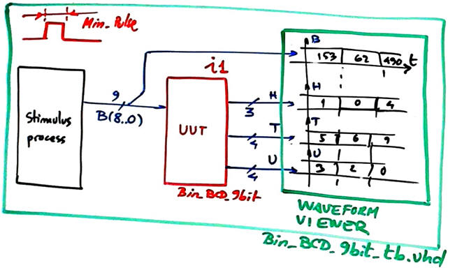
Test bench schematic for validating our design is always the same, as represented in Fig. 7.
 |
|
Fig. 7. Testbench fixture to check the unit under test. |
Fig. 2 timing diagram can be translated to a VHDL testbench process. An example test bench Bin_BCD_9bit_tb.vhd from where to copy and adapt vector stimulus input signals and constant Min_Pulse.
Run the VHDL simulation EDA tool to obtain and discuss the timing diagram.
|
|
|
Fig. 8. Example testbench showing ideal results. |
5. Testing at the gate-level the technology schematic to measure circuit's speed
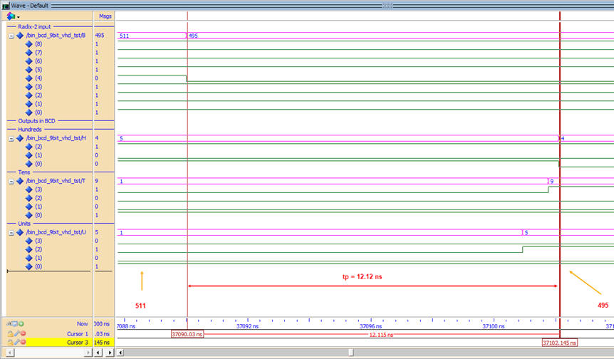
Using a gate-level simulation is possible to measure propagation delays at a given signal transition. How long does it take to propagate signals from a given switching input to an output?
 |
|
Fig. 9. Example testbench showing real results in a specific signal transition from B = 511 to B = 495. |
Using the timer analyser tool is possible to measure the worst-case propagation time scenario, and thus determine the maximum circuit's speed for processing 9-bit code conversions.
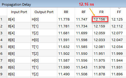 |
Fig. 10. Timing analyser estimating the worst-case scenario on propagation delay: when the input B(4) switches from '1' to '0' (falling transition) and the output H(0) goes from '0' to '1' (rising transition) there is the maximum propagation time of 12.16 ns. This means that this circuit can calculate 82.23 millions of code translations per second. |
6. Report
At least five handwritten sheets of paper as usual in CSD. Follow this rubric for writing reports.
7. Prototyping
Use training boards and perform laboratory measurements to verify how the circuit works. For instance, Fig. 11 shows the theoretical waveforms running near the minimum period when switching two truth table values. Propagation time estimation is from the timing analyser in Fig. 10.
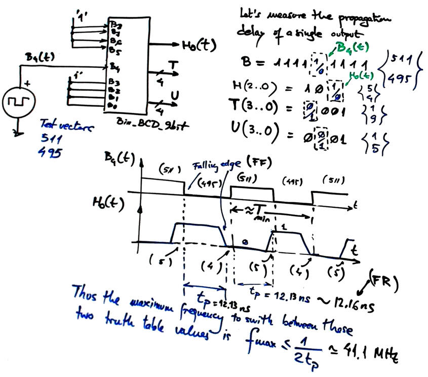 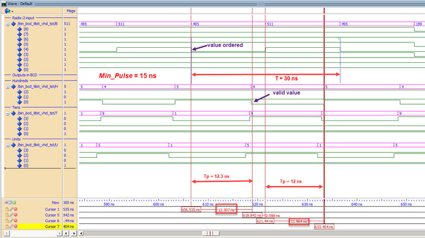 |
Fig. 11. Sketch of the instrument fixture for propagation delay measurements considering a single input and output waveforms. Input is switching from B = 511 to B = 495. Simulations shows values near the limit Tmin. |
| Home Term 26/27-Q1 Contact Products Electronic devices and companies Software Books Magazines Instruments DEE Library EETAC DEEL |

|
|
| Web activa des de 09/2001, @ F. J. Robert, Web editat amb Microsoft Expression Web 4. El contingut és un complement als materials d'estudi del curs Circuits i Sistemes Digitals disponibles al campus digital Atenea. Llicència:Reconeixement 4.0 Internacional de Creative Commons |