|
|
Bachelor's Degree in Telecommunications Systems and in Network Engineering |
|
|
|
||
|
|
Comp_4bit plan A: structural equations single-file VHDL |
|
|
|
||
4-bit expandable comparator using equations
1. Specifications
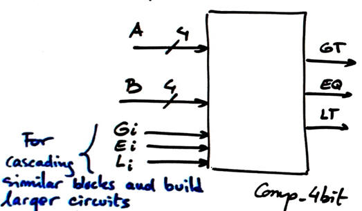
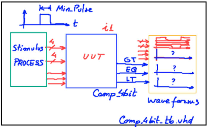
Design a 4-bit expandable comparator Comb_4bit using plan A: flat structure based on equations deduced from the circuit's truth table.
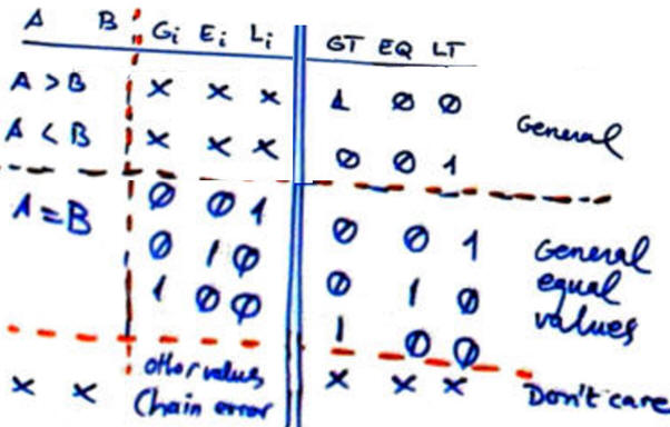
Comp_4bit has the symbol and truth table represented in Fig. 1. A chip of this kind is the 74LS85.
|
|
| Fig. 1. Symbol and truth table of a 4-bit comparator with extra signals for expandability. |
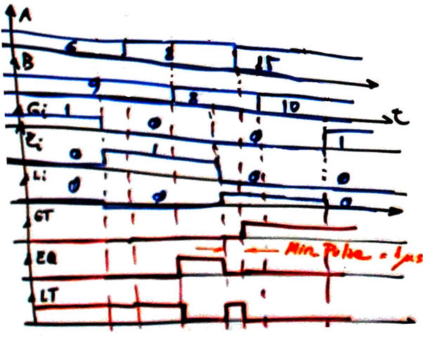 |
| Fig. 2. Example of timing diagram. Outputs are deduced from the circuit's truth table. |
2. Planning
This time the circuit's truth table is 2^11 = 2048 combinations, thus not practical for deducing maxterms or minterms, and also not practical for writing a compact table in minilog. Let us try to deduce circuit's equations simply inspecting the truth table and considering numeric examples. A and B are radix-2 (weighted code) 4-bit numbers.
Therefore, we will take advantage of the many "don't care" terms considering that we have got weighted codes. Additionally, GT, LT and EQ are incomplete functions with many output values of no interest, for instance when Gi = '1' and Ei = '1', outputs are of no interest. This book is a reference: Ercegovac, M., Lang, T., Moreno, J. H., "Introduction to Digital Systems", John Wiley & Sons, 1999). It includes slides: Chapter 10 is on arithmetic circuits where this set of equations are deduced.
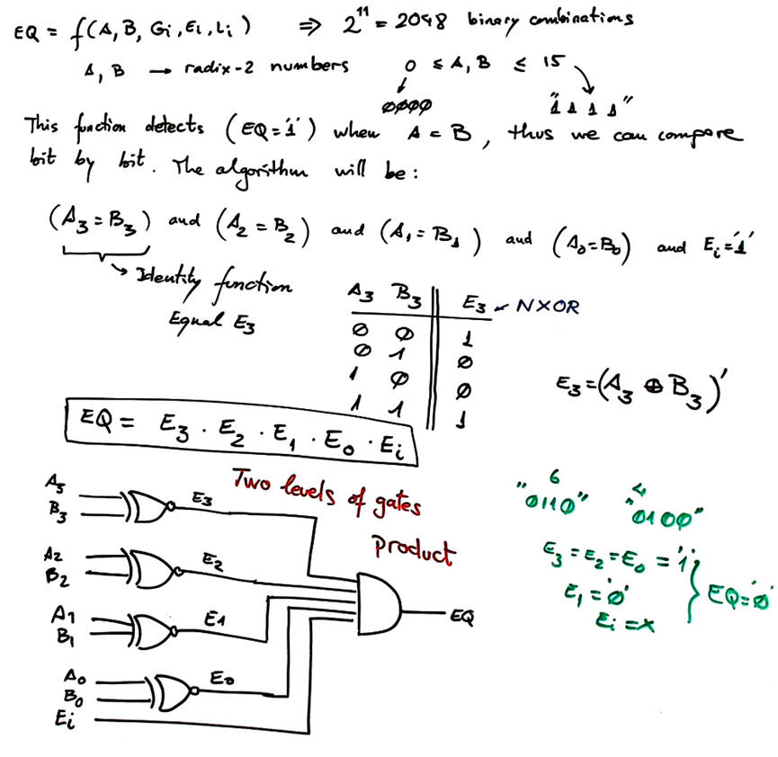 |
Fig. 3. Deducing output EQ. |
EQ requires two levels of gates AND and NXOR.
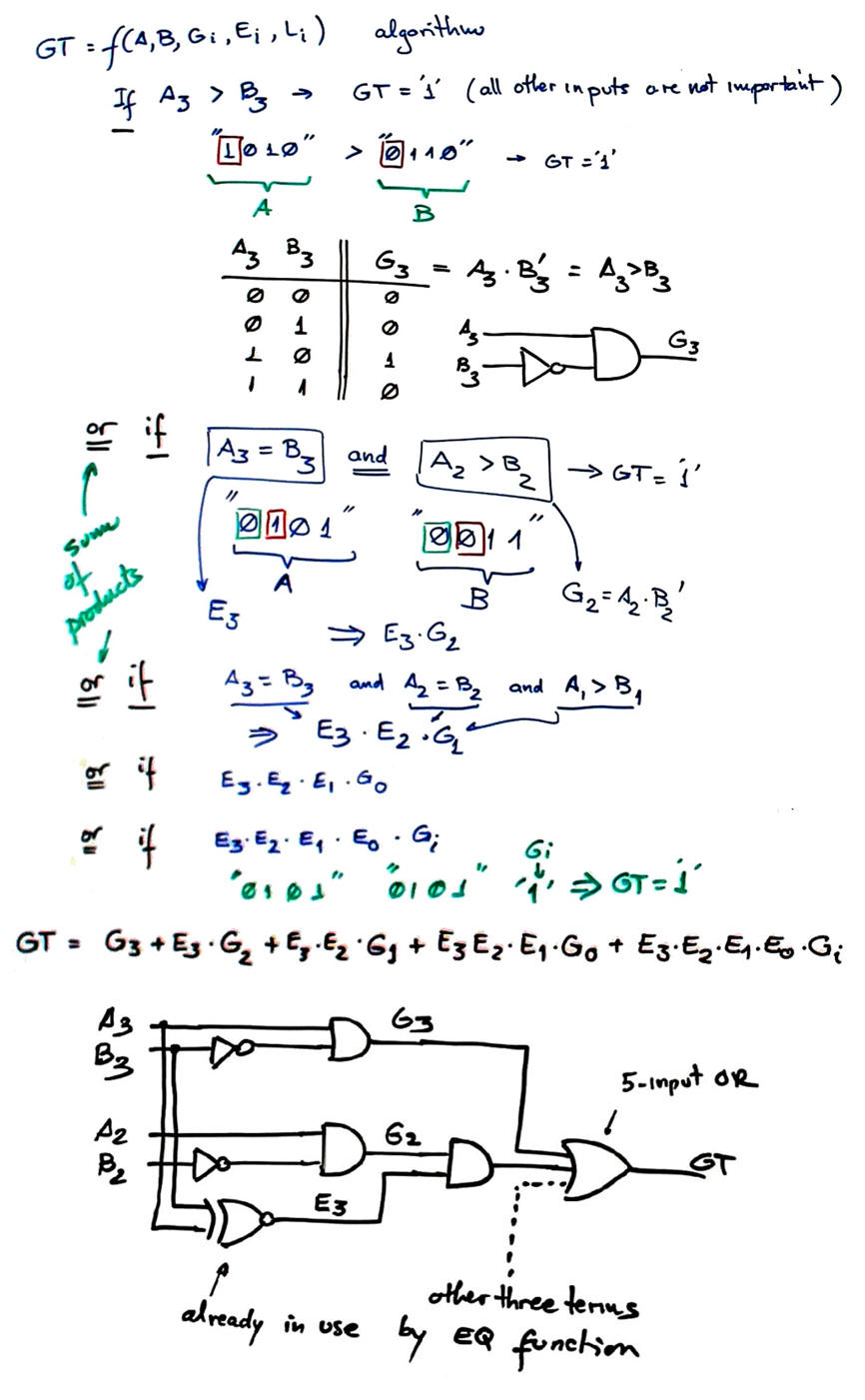 |
Fig. 4. Deducing output GT. |
GT requires 4 levels of gates, considering that NXOR gates can be used again now.
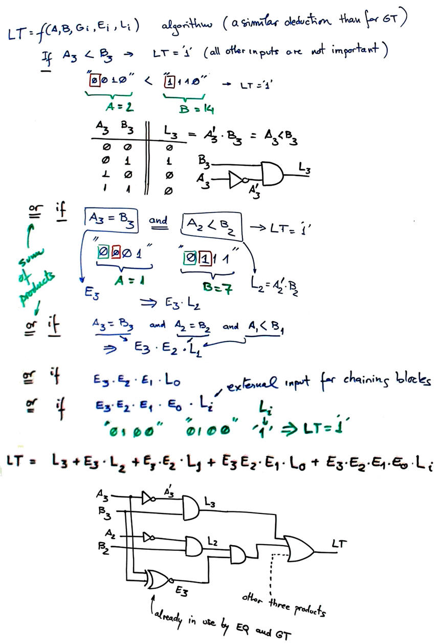 |
Fig. 5. Deducing output LT. |
Project location:
C:\CSD\P3\Comp_4bitA\(files...)
Note: The same component Comp_4bit is designed using plan C2 strategy consisting of chaining Comp_1bit components. Thus, a good exercise here is to compare both solutions and discuss questions related to circuit optimisation, such:
-
What plan is faster (computes more 4-bit numbers comparisons per second?
-
What plan is requires less resources (logic gates or logic cells)?
-
What plan is simpler to infer and comprehend?
-
What are the limitations of this plan A when expanding the algorithm to 5 or 6 bit numbers?
3. Developing the project using EDA tools
This is the 4-bit comparator Comp_4bit.vhd that corresponds exactly to the translation of equations discussed above.
Run a EDA project to synthesise the circuit. Select a target chip like Intel Cyclone IV EP4CE115F29C7.
Fig. 4 shows an example of RTL schematic generated after the synthesis process.
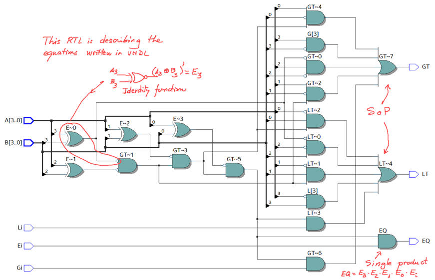 |
| Fig. 4. RTL view from Intel Quartus Prime. |
 |
|
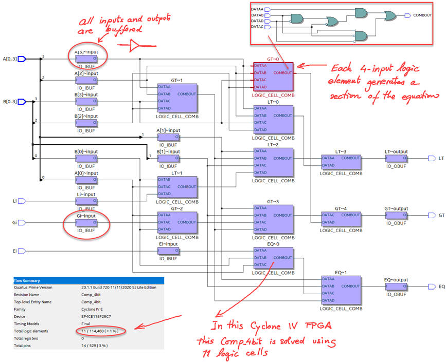
Fig. 5. Example technology view for a Cyclone IV FPGA chip. |
How many resources (logic elements) are used? 11 logic elements, from the synthesis summary or from the technology view. In this FPGA cyclone IV, each logic element is used as a 4-input combinational block.
4. Testing and validating the design
The VHDL testbench schematic for validating our design is always the same. We apply a sequence of stimulus input vectors, and run the simulations for obtaining time results in a kind of logic analyser representation.
 |
|
Fig. 6. Testbench fixture. |
Fig. 2 timing diagram sketch can be translated to a VHDL testbench process. An example test bench Comp_4bit_tb.vhd from where to copy and adapt vector stimulus input signals and constant Min_Pulse.
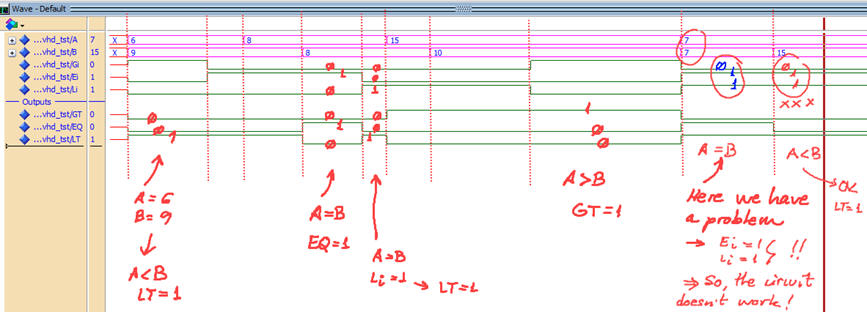
Run the VHDL simulation EDA tool to obtain and discuss the timing diagram.
 |
|
Fig. 7. Example testbench showing ideal results. |
5. Testing at the gate-level the technology schematic to measure circuit's speed
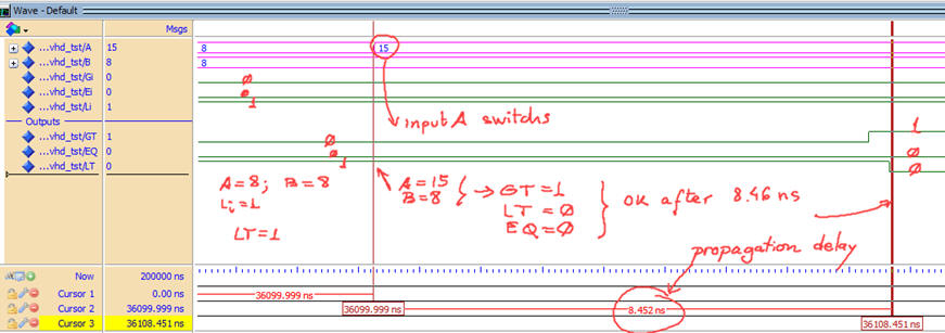
Using a gete-level simulation is possible to measure propagation delays at a given signal transition. How long does it take to propagate signals from a given switching input to an output?
 |
|
Fig. 8. Example testbench showing real results in a specific signal transition. |
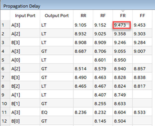
Using the timer analyser tool is possible to measure the worst-case propagation time scenario, and thus determine the maximum circuit's speed when processing comparisons. In Fig. 9 we observe that the longest propagation delay of tP = 9.5 ns happens when A(3) input is falling anf the LT output is rising. It means that this Cyclone IV can perform fMAX = 105.2 MHz (105 millions of 4-bit comparison operations per second), thus, the minimum Min_PulseMIN = 10 ns. If the circuit is switching faster than Min_PulseMIN digital outputs are not generated.
 |
|
Fig. 9. Timing analyser estimating the worst-case scenario on propagation delay. |
6. Report
At least five handwritten sheets of paper as usual in CSD. Follow this rubric for writing reports.
7. Prototyping
Use training boards and perform laboratory measurements to verify how the circuit works.
| Home Term 26/27-Q1 Contact Products Electronic devices and companies Software Books Magazines Instruments DEE Library EETAC DEEL |

|
|
| Web activa des de 09/2001, @ F. J. Robert, Web editat amb Microsoft Expression Web 4. El contingut és un complement als materials d'estudi del curs Circuits i Sistemes Digitals disponibles al campus digital Atenea. Llicència:Reconeixement 4.0 Internacional de Creative Commons |