|
|
Bachelor's Degree in Telecommunications Systems and in Network Engineering |
|
|
Gate-level VHDL simulation and timing analyser |
||
ModelSim Intel Edition Xilinx ISim ActiveHDL Lattice Edition
The idea is to verify a digital circuit synthesised in a PLD (CPLD or FPGA), emphasising the measurement of propagation delays at a given signal transition.
Firstly, accordingly to our VHDL design flow, once a circuit has been synthesised for a given target chip, a functional simulation has been carried out in order to validate the ideal circuit (RTL view).
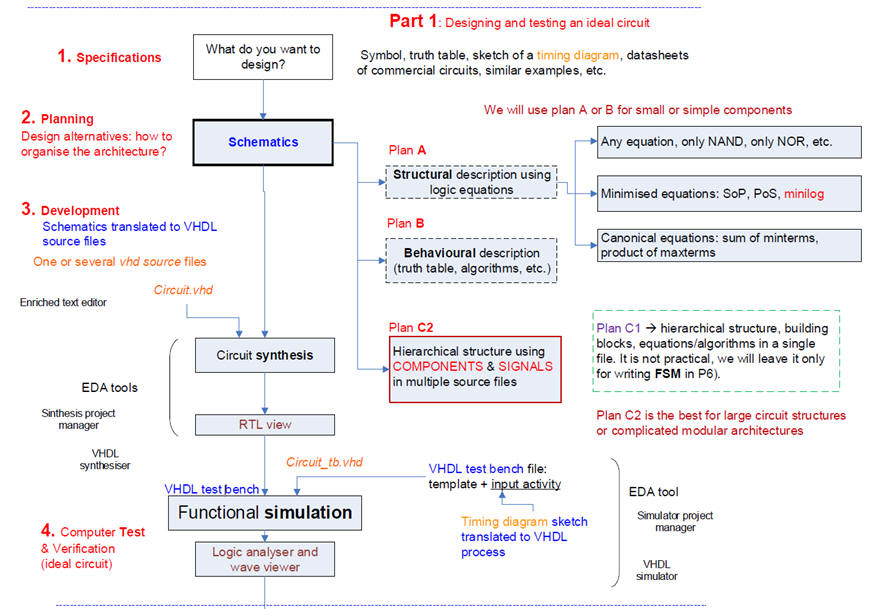 |
Fig. 1. VHDL design flow used in CSD. |
Secondly, it is necessary a verification of the real circuit (technology view), and thus, gate-level simulations including propagation delays and other constraints associated to a given technology or device. Technology evolve over time and digital circuit become better and better solving logic functions with less power consumption and higher speed of computation.
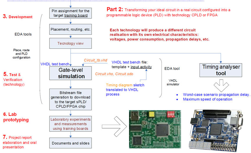 |
Fig. 2. Second part of our design flow involving two new tools: gate-level simulations and timing analyser. |
Therefore, we have to add the 5th step: a gate-level simulation of a real circuit synthesised specifically for a given PLD target chip. We will examine how circuits behave in specific signal transitions as if we were using a laboratory logic analiser instrument.
Finally, using the timing analyser tool, let us calculate the longest input-output signal path that will generate the worst-case scenario: the maximum propagation delay, and thus measure the maximum speed of processing for a given target chip.
The purpose of this tutorial is to exemplarise the gate-level simulation process. The EDA tools are installed and available in your portable computers (rec.)
1. Project specifications; 2. Planning; 3. Project development and circuit synthesis
Let choose the 8-bit integer adder/subtractor Int_add_subt_8bit as the example circuit to validate using a VHDL testbench.
These are the VHDL files defining the hierarchical project to be the device-under-test (DUT) represented in Fig. 3: Adder_1bit.vhd, Adder_4bit.vhd, Adder_8bit.vhd, Int_add_subt_8bit.vhd. Let's go step by step.
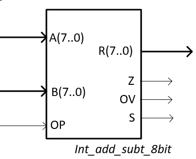 |
Fig. 3. Entity under design. |
Circuit design
1. Start a project to synthesise the circuit.
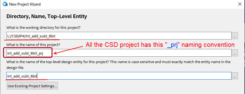 |
Fig. 4. Project name and location. |
2. Select all the files attached to the hierarchical architecture.
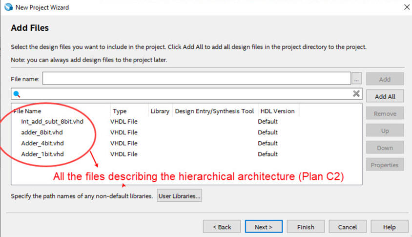 |
Fig. 5. Include all components in the design. |
3. Select the target chip to be used in this free edition of Quartus Prime. For instance the Cyclone IV FPGA populating the DE2-115 board from Terasic.
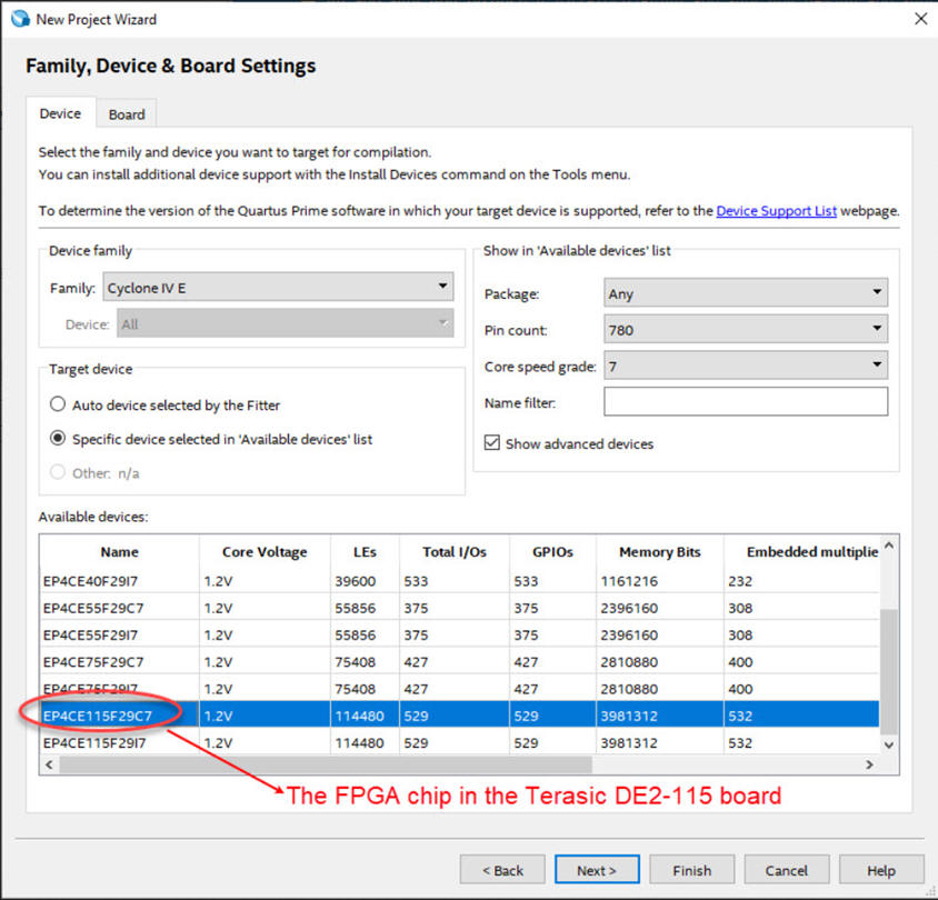 |
Fig. 6. Target chip aimed for the synthesised design. |
4. Select the simulation tools: ModelSim Intel Starter Edition.
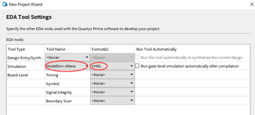 |
Fig. 7. Select the tool for VHDL simulations. |
5. The RTL schematic is represented in Fig. 8. It has to be inspected from the top to bottom verifying that it corresponds to what we described in VHDL as the translation of our sketched plan.
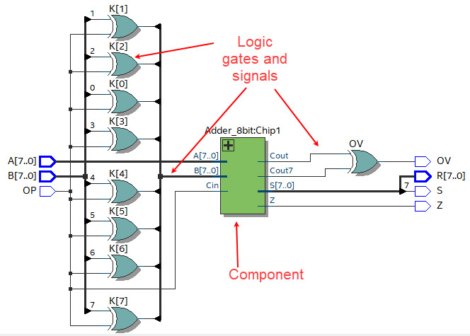 |
Fig. 8. RTL schematic generated by Quartus Prime. |
You can also inspect the technology view and check that some logic elements are used for implementing the circuit logic functions (represented in Fig. 15).
4. Functional simulation
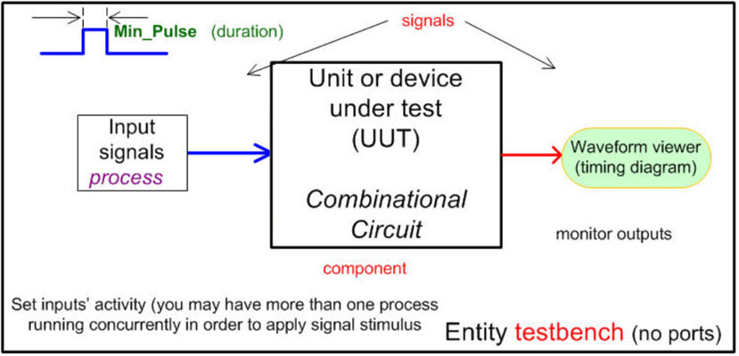
This is the VHDL testbench fixture and concept. For simple circuits we'll place all the stimulus signals in a single process.
 |
|
Fig. 9. The idea of a VHDL testbench. |
6. Generate the testbench template which will be copied to the project folder and renamed.
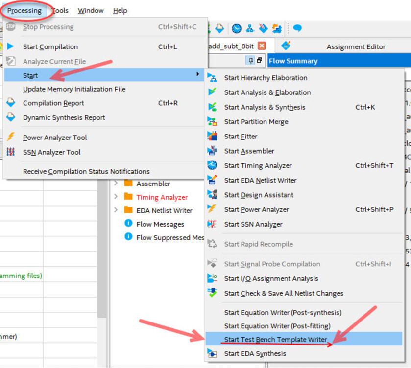 |
Fig. 10. This is how to order a VHDL testbench template or skeleton. |
7. This is an example testbench Int_add_subt_8bit_tb.vhd containing some stimulus translated from the timing diagram sketch in our specifications.
8. Lauch ModelSim Intel Edition from the Quartus environment or from Windows and start a new project. It has to be placed in the project folder along with the other files defining the entity.
C:\CSD\P4\Int_add_subt_8bit\
 |
Fig. 11. Two ways to launch ModelSim: from Quartus Prime when configured, and from the Windows application. |
9. Add the files that conform the architecture and the testbench; compile all and start a functional simulation.
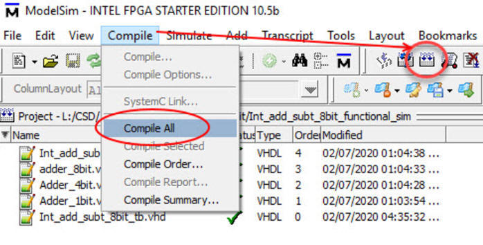 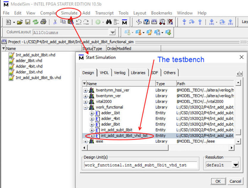 |
Fig. 12. Add all files, compile and start a functional simulation. |
10. Run enough time to include all vectors written in the stimulus process. For instance, in this example Min_Pulse constant is set to 15.25 μs, thus running 2000 μs is enough.
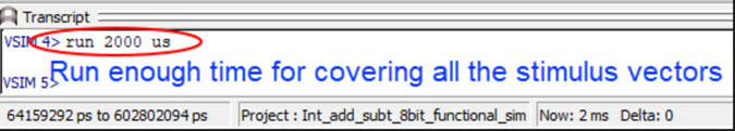 |
Fig. 13. Run the simulations enough time. Real time is related to Min_Pulse constant. |
The simulation results are represented in Fig. 14 timing diagram (wave diagram).
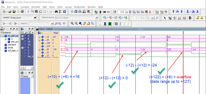 |
Fig. 14. Timing diagram showing some stimulus and results from the functional simulation. |
These steps from 1 to 10 cover the typical design process: specify, plan, develop, test in order to verify that our circuit works as expected, meaning that we can validate some values of the truth table by observing the waves. Naturally, in VHDL an automatic validation of all the truth table is possible, but out of the scope of this CSD course (131072 combinations in this circuit).
Gate level simulation using Quartus Prime and ModelSim Intel Edition
5. Gate-level simulation and timing analyser
Our objective is measuring propagation delays in signal transitions. Let us use the same testbench and EDA tools. However, this time we will simulate the real circuit configured in the FPGA fabric, it will be translated to VHDL along with the standard delay output file associated to the target chip.
For instance, the Cyclone IV FPGA EP4CE115F29C7 populating the DE2-115 board from Terasic. Examine the technology in Fig. 15.
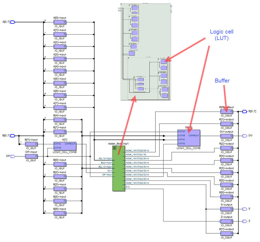 |
Fig. 15. Technology circuit implemented in the FPGA. |
11. Generate the VHDL description of the schematic (Int_add_subt_8bit.vho) which uses the file extension VHO launching the EDA netlist writer.
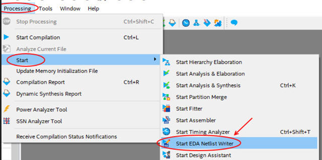 |
Fig. 16. How to generate the VHDL translation of the technology schematic. |
And also generate the SDO (standard delay output file, Int_add_subt_8bit.vhd.sdo). Be sure that the project EDA tool settings netlist writing are all set to Off.
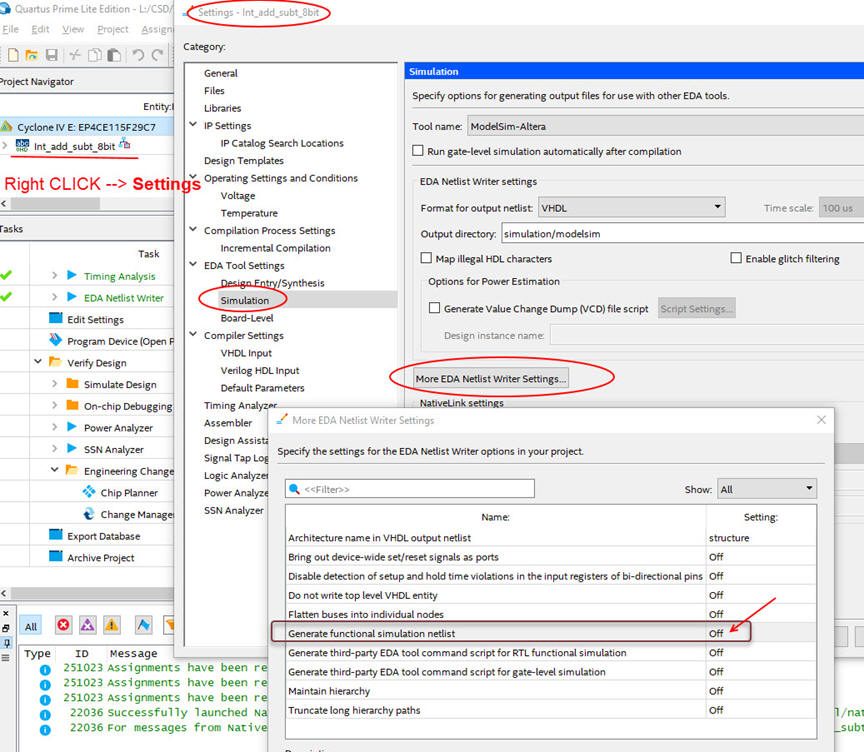 |
Fig. 17. Settings for generating the standard delay file. |
12. From Quartus Prime (or from the Windows application) start a new gate-level simulation project in ModelSim Intel Edition.
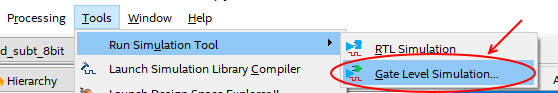 |
Fig. 18. Start a new ModelSim project |
Location: C:\CSD\P4\Int_add_subt_8bit\
Project name: Int_add_subt_8bit_gate_level_sim
Library: Work_gate_level
13. Adding existing files: the testbench: Int_add_subt_8bit_tb.vhd, and the technology file: Int_add_subt_8bit.vho
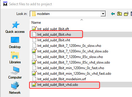 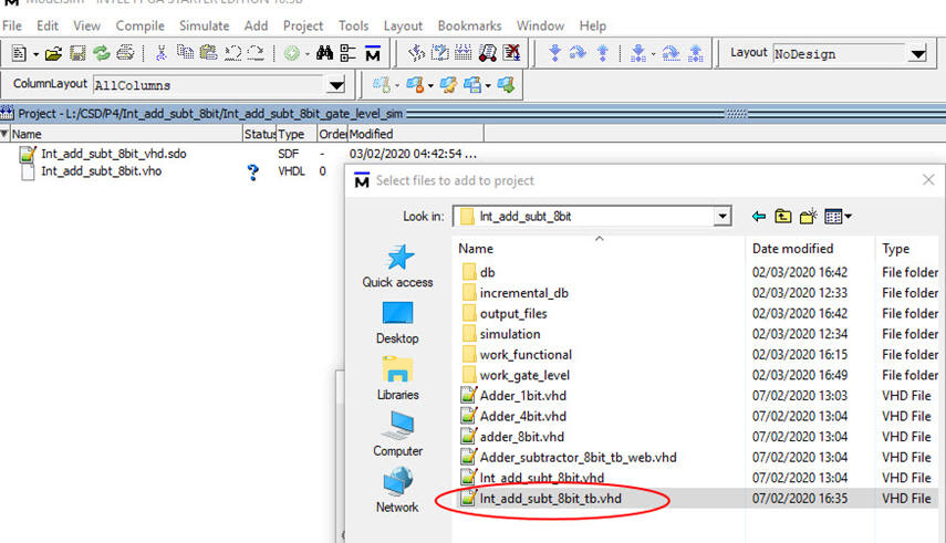 |
Fig. 19. Add the technology file (vho) and the testbench (delay file will be added later). |
14. Start the simulation. First step is selecting the top entity name: int_add_subt_8bit_vsd_tst in the testbench file.
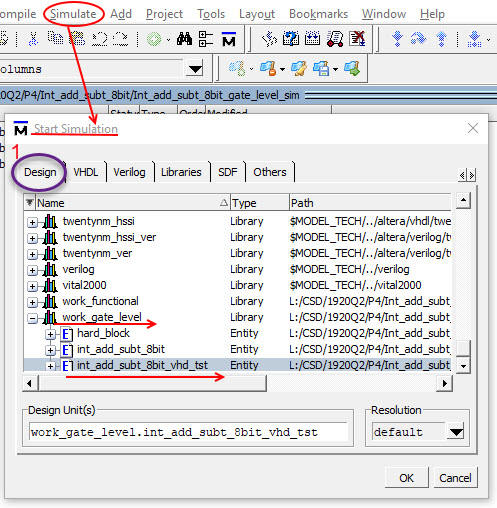 |
Fig. 20. Select the top entity to simulate (the testbench) |
15. Start the simulation. Second step is attaching the timing constrains, the SDF file, to the region entity (i1) or device under test, in the testbench.
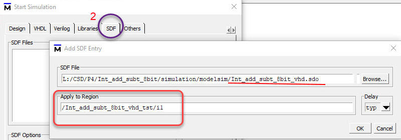 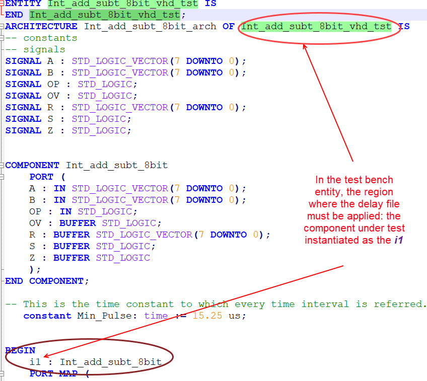 |
Fig. 21. Region where to apply the SDO file. |
16. Add a wave diagram and all the signals of interest in the region, and run.
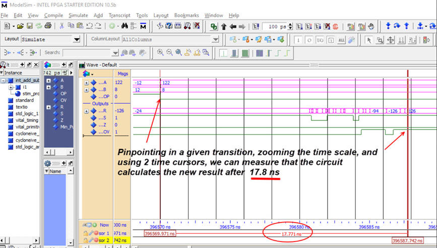 |
Fig. 21. Wave diagram showing a zoomed transition where to make measurements of propagation time |
The propagation delay measurement shows that it takes about 18 ns from switching the input OP and getting the right output OV value.
Timing analyser
We can find the worst-case scenario using Quartus Prime timing analyser: Which is the longest propagation delay?
17. Launch the timing analyser tool from the Quartus prime.
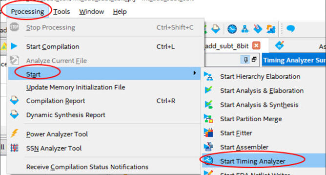 |
Fig. 22. Starting the timing analyser tool. |
18. Use the timing analyser to see the datasheet spreadsheet for propagation delays.
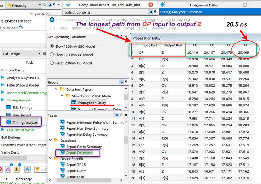 |
Fig. 23. Worst case calculations scenario involving the longest path from input to output or the larger number of gate levels. |
And from results in Fig. 23, it can be deduced the maximum speed of computing 8-bit integer additions and subtractions for this target chip and the hierarchical structure proposed: tP = 20.47 ns from OP to Z; maximum speed is 1/tP = 48.85 mops; and finally, the maximum frequency of a digital generator driving OP is: fmax <= 1/(2·tP) = 24.4 MHz.
Gate level simulation using Xilinx ISim
5. Gate-level simulation using Xilinx ISim
Gate level simulation ActiveHDL Lattice Edition
5. Gate-level simulation using ActiveHDL Lattice Edition
| Home Term 26/27-Q1 Contact Products Electronic devices and companies Software Books Magazines Instruments DEE Library EETAC DEEL |

|
|
| Web activa des de 09/2001, @ F. J. Robert, Web editat amb Microsoft Expression Web 4. El contingut és un complement als materials d'estudi del curs Circuits i Sistemes Digitals disponibles al campus digital Atenea. Llicència:Reconeixement 4.0 Internacional de Creative Commons |