|
|
Bachelor's Degree in Telecommunications Systems and in Network Engineering |
|
|
|
||
|
|
Adder_4bit ripple-carry. Plan C2: hierarchical multiple-file VHDL |
|
|
|
||
4-bit adder circuit based on ripple-carry technique
1. Specifications
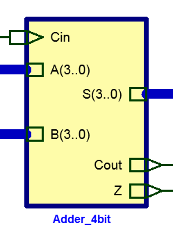
Design a 4-bit adder (Adder_4bit) using a ripple-carry hierarchical structure based on multiple components (plan C2). In Fig. 1 there is the circuit's truth table, and this is the algorithm: S = A + B + Cin.
With the purpose of practising plan C2, the circuit contains an extra output Z, a flag or indicator, that detects when the result is zero.
 |
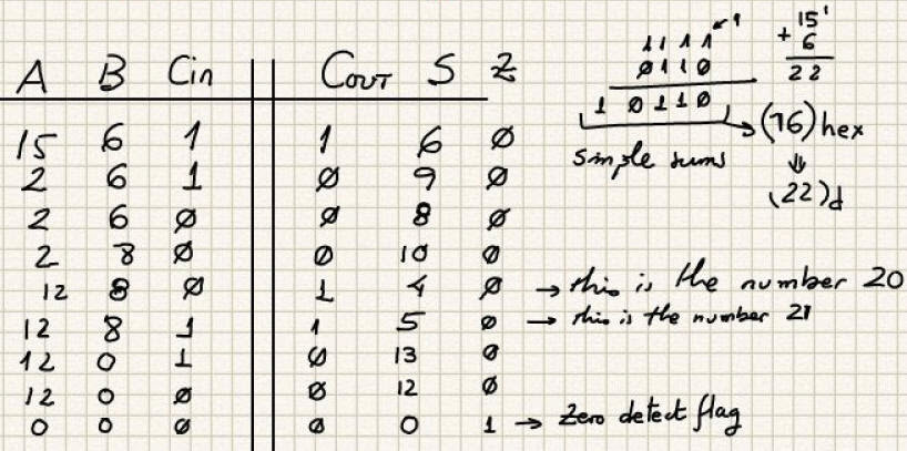 |
| Fig. 1. Symbol and truth table. We use radix-2 unsigned numbers better than '0' and '1' for data inputs and outputs. |
Fig. 2 is an example of timing diagram representing some circuit's operations.
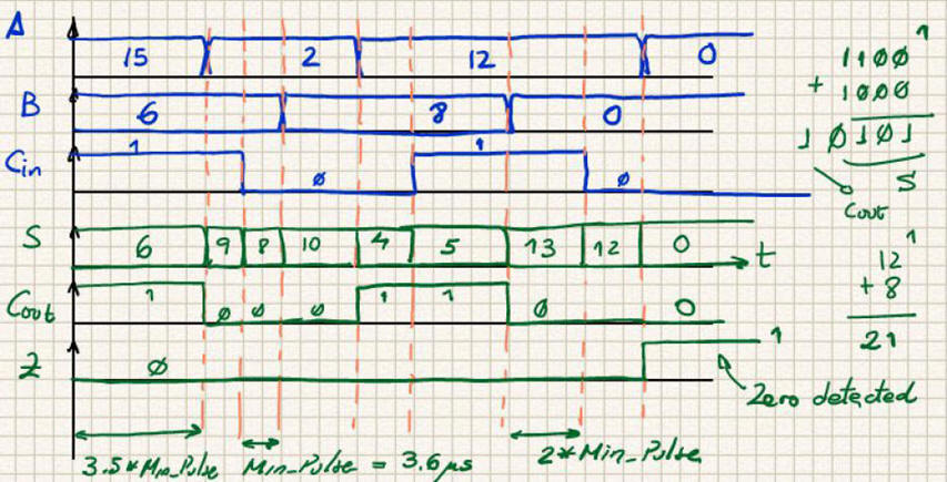 |
| Fig. 2. This is an example of a timing diagram representing some operations. |
2. Planning
Structural and hierarchical plan C2 based on the ripple-carry technique: the 4-bit adder is generated chaining 1-bit full adder components. The proposed architecture is represented in Fig. 3. Thus, the project will become a multiple-file hierarchical VHDL project. The top entity Adder_4bit and the component Adder_1bit used up to 4 times.
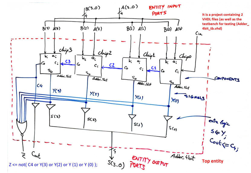 |
| Fig. 3. Adder_4bit modular hierarchical architecture. |
Some questions that may be of your interest:
-
How many COMPONENTS and how to connect them?
-
How many SIGNALS and how to name them?
-
Do you see the difference and how to handle a simple 1-wire STD_LOGIC and a n-wire STD_LOGIC_VECTOR(n-1 downto 0)?
-
Do the circuit require extra circuits like logic gates?
-
How to connect them?
-
How many VHDL files you need for this project?
-
Why are buffer gates such as Cout <= C4 required?
-
Which is the project name and the name of the top entity?
-
Where to find and copy the component Adder_1bit?
-
Where to find a similar circuit based on plan C2 to copy & adapt to be our Adder_4bit?
-
Are there alternative plans such as carry-lookahead (CLA) that offers some advantages? (see this other version of Adder_4bit).
This approach is also an answer to the question: "How to expand it?" in our concept map: How to expand an Adder_1bit to build for example an Adder_16bit?
Project location:
C:\CSD\P3\Adder_4bit_RC\(files)
3. Developing the project using EDA tools
Plan C2. Structural. This is the VHDL file top entity represented in Fig. 3: "Adder_4bit.vhd".
And now the component Adder_1bit. You can use different plans to implement this component and obtain its VHDL file, all of them independent projects reported in several tutorials. For instance:
- Plan A) Adder_1bit. You will find several equations from A1 to A7.
- Plan B) Adder_1bit. Directly interpreting the truth table.
- Plan C2) Adder_1bit It is Implemented using the MoD.
- Plan C2) Adder_1bit (LAB3) It is Implemented using the MoM
NOTE: : This is the important goal in this tutorial on Plan C2: how to translate hierarchical schematics into a multiple file VHDL projects. Print the sheets (1) and (2) ) and annotate whatever is meaningful for you in this translation process. We will repeat the same procedure once and again from now on to translate a Plan C2 into VHDL files for whatever application.
Select a target chip chip, for instance the MAX II EPM2210F324C3 from Intel. Run a new EDA project adder_4bit_prj to synthesise the circuit including the necessary VHDL files.
Fig. 4 is an example of RTL schematic for this hierarchical project.
|
|
|
Fig. 4. RTL view of Adder_4bit structure once synthesised using EDA tools. The Adder_1bit component is solved using plan A equations. |
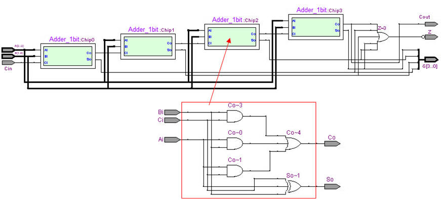
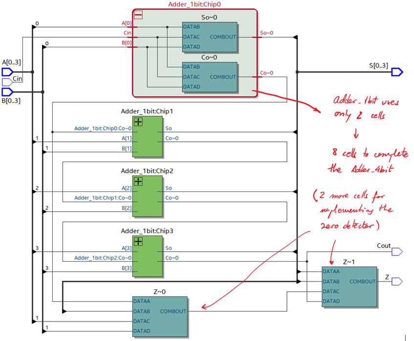
Fig. 5 is an example of technology view when selecting a MAX II chip EPM2210F324C3 from Intel.
|
|
|
Fig. 5. Technology view. How many resources are used in this design (logic elements)? The chain of Adder_1bit requires 8 cells, and the implementation of Z output another 2 cells. |
4. Testing and validating the design: functional VHDL simulation
Fig.6 is the representation of the VHDL testbenchfixture. Those are the concepts and ideas in mind and paper.fixture. Those are the concepts and ideas in mind and paper.
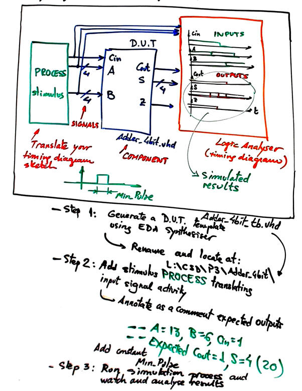 |
| Fig. 6. Example of VHDL testbench schematic and sequence of operations to complete a simulation. |
From an initial VHDL test bench Adder_4bit_tb.vhd, simply copy the constant n_PulseMin_Pulse and the stimulus process to your template.
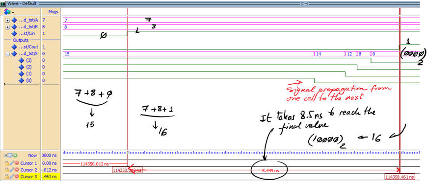
Start a new ModelSim simulation project and run to obtain and discuss the timing diagram. This is an example of resulting waveforms.
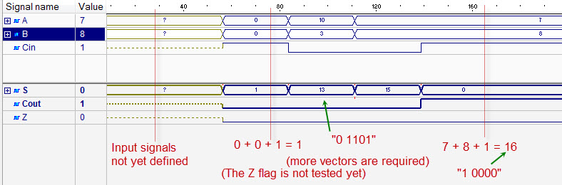 |
Fig. 7. Example of a test results. |
5. Testing and validating the design: gate-level VHDL simulation
Use the same testbench file from the functional simulation. Run a gate-level simulation project in ModelSim to observe signal propagation.
 |
| Fig. 8. Example of gate-level results when the circuit is implemented in a MAX II from Intel. |
Calculating tP. Run the Quartus Prime timing analyser tool to obtain the worst-case scenario: the largest signal path and so the longest propagation time from inputs to outputs ( tP).
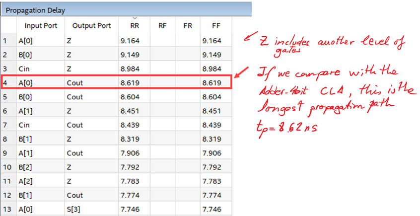 |
| Fig.9. Timing analyser results. In this example the longest signal propagation path is from A(0) to Cout, representing tP = 8.62 ns. From this measurement we deduce what is the theoretical maximum operating frequency of this circuit, representing as well the minimum value permitted for Min_Pulse, or the maximum ratio at which inputs can be switched for a given target chip. In this case speed = 1/tP < 116 Mops (millions of operations per second). |
It is time to compare both implementations of the same circuit: (1) this ripple-carry Adder_4bit and (2) CLA Adder_4bit . Which one is faster? Which one uses more resources? Perhaps, to better characterise ripple-carry and carry-lookahead adders we need more bits. In LAB4.1 the Adder_16bit is studied using both architectures.
6. Report
Follow this rubric for writing reports.
7. Prototyping
Use training boards and perform laboratory measurements to verify how the circuit works
| Home Term 26/27-Q1 Contact Products Electronic devices and companies Software Books Magazines Instruments DEE Library EETAC DEEL |

|
|
| Web activa des de 09/2001, @ F. J. Robert, Web editat amb Microsoft Expression Web 4. El contingut és un complement als materials d'estudi del curs Circuits i Sistemes Digitals disponibles al campus digital Atenea. Llicència:Reconeixement 4.0 Internacional de Creative Commons |