|
|
Bachelor's Degree in Telecommunications Systems and in Network Engineering |
|
2021Q2 - Laboratory projects
NOTE: VHDL EDA in use: Intel Quartus Prime Lite, ModelSim Intel Edition, Proteus electrical simulator, minilog minimiser, notepad++ editor, Microchip MPLABX and XC8 compiler.
NOTE: For all projects, labs and tutorials, do not invent or change the name of a file, folder, component, signal, etc. that are given to you in schematics, diagrams or explanations. All the names and features are carefully selected and annotated to make it easy to solve our projects in the given study time. If you have the need to invent a name, for instance to translate to VHDL a plan C2 circuit, don't do it, please, ask questions instead to get help and solve your doubts. This is our way to save you countless unproductive hours.
P_Ch1 designing an arithmetic and logic circuit using hierarchical multipl-file plan C2
Assignment. Due date April 8th. Questionnaire Q1_4 by April 8th
This is an example of operations to be performed by ALU_9bit and also a way to comprehend the meaning of the input vectors in context of the operation under execution (information or data processing).
Assignment. Working assessment March 8th.
Assignment. Working assessment March 15th.
Assignment. Working assessment March 22nd.
|
NOTES: - VHDL files are not assessed because what is of interest are schematics, flowcharts, sketches, diagrams, etc. that you prepare carefully with annotations and explanations all over project sections. In our introductory CSD course, VHDL files are required simply as straightforward translations of such schematics and flowcharts. Thus, do not write VHDL without a plan. - Never change the name of the entity, because other names are invalid. This circuit is named Adder_2bit. - Entity description is always the same, whatever the plan you are intended to use as architecture. - Be aware of what is a single wire such Cin, and what is a vector wire (cable) such S(1..0). Ports are represented in the circuit's symbol and described in the entity. - Never copy and paste files from your colleagues; it has no meaning, like cheating, unfair, it is completely useless, you are not learning properly and thus, you likely fail exams. - Never mix your materials, but use different folders to develop and save project information and files. For instance: L:\CSD\P_Ch1\SP1_3\Adder_2bit_A\(files) L:\CSD\P_Ch1\SP1_3\Adder_2bit_B\(files) - Do not start trying to solve the Adder_2bit, but instead study, run and analyse how other tutorials examples are functioning. For instance, if you have interest in solving a circuit using flat behavioural method plan B, investigate firstly projects such: Hex_7seg_decoder plan B Dec3_8 plan B MUX_8 plan B, (with up to four different flowcharts or schematics) Adder_1bit plan B Comp_1bit ideas using plan B -Be aware that CSD lab projects are completely related to the whole course; when solving lab projects you learn the full subject and in this way you can obtain good marks in questionnaires and exams. |
This assignment is intended to put into practice hierarchical design (plan C2) and be able to finish P_Ch1 using the proposed architecture below based on interconnecting several components:

This is the way Arith_9bit data must be interpreted when operating. Solve several operations of the circuit's truth table to comprehend correctly the data organisation.

Thus, you better follow this sequence to complete the lab project:
1) Invent Chip_2 component Comp_9bit as stated in the assignment : I - II - III - IV.
Here there is a new video rec. on Adder_2bit from SP1_3 using now plan C2 that is of your interest.
2) Invent Chip_1 component Sel_Add_Subt_9bit using hierarchical architectures similar to P3 and P4. The picture below shows you some ideas and planning. One option is to build the component Adder_9bit using your previous designs from SP1_2 and SP1_3. Pay attention that you must include Cout8 as a port to be able to generate OV flag function.

3) Invent Chip_3 component. You can choose plan C2 or plan B for the Triple_MUX_2.
4) Assemble all the blocks, develop and test the complete Arith_9bit. Run several operations from its truth table to demonstrate that it works as expected.
|
|
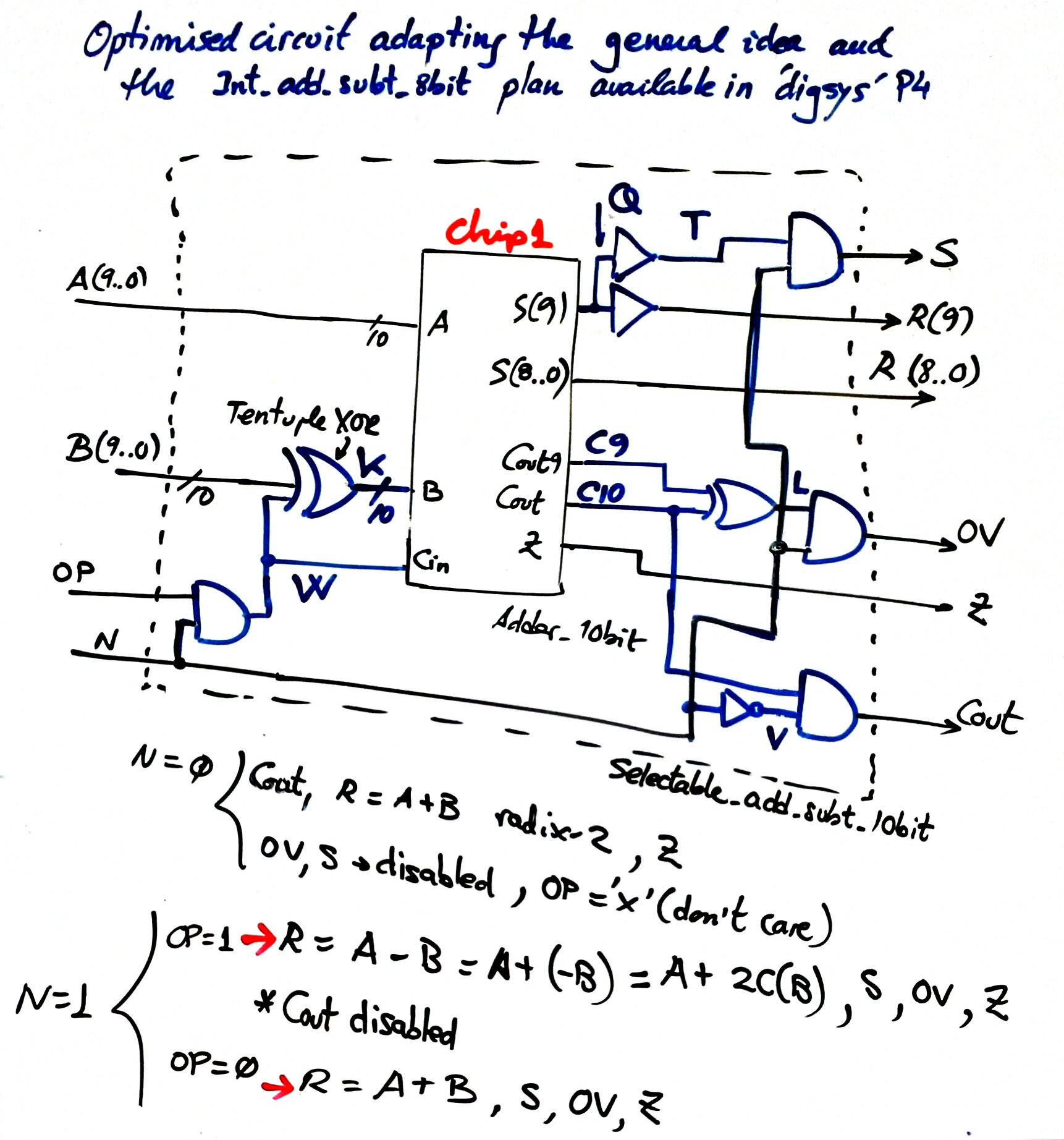
This is yet another convenient project Selectable_add_subt_12bit circuit from former 1920Q2. Input N decides which data type to add or subtract: natural or integer numbers. Conceptual idea on designing a circuit for several operations, a plan and video rec. on how to translate such plan into a VHDL equivalent file for developing the project.
|
|
P_Ch2 designing sequential systems: programmable timer
Assignment. Due date May 17th. Questionnaire Q5_8 by May 19th. This is our dedicated processor:

Assignment on circuit's speed measurements. Working assessment April 26th.
For instance, this is a plan C2 to build the Comp_24bit required in P_Ch2 datapath (SP2_4).

Assignment. Working assessment May 3rd.

As usual in CSD, before starting, and also for preparation of cooperative group work, try to organise your project in a mind map. In this way, all the queries and questions will be referring to a given process, method or solution step, for instance:

-
SP2_3 Implementing FSM
Assignment. Working assessment May 10th.


Question: How to write the testbench for the Prog_Timer?
Firstly, draw your timing diagram in paper as we did for instance in P_Ch2 Fig. 1 immediately below the symbol. Think what are you going to do with input signals for the complete Prog_Timer in time to demonstrate that it works. Do not forget that your VHDL testbench with stimulus is ONLY a translation of such handwritten timing diagram. Prepare your CLK, prepare your CD pulse, prepare your PC value, and finally prepare your TRG pulse, and infer and discuss what is going to happen with circuit outputs as long as time is advancing.
Secondly, get the testbench skeleton for the Prog_Timer from Quartus Prime and draw the testbench fixture, something like this picture below, in this way you know in advance always what is going on and what you are expecting from VHDL simulations:

Thirdly, translate your inputs signals in VHDL processes (one at a time if you like) the same way we do all the time and run a functional simulation. Is your result pretty much like your timing diagram?
Question: How to prepare the video recording?
The idea of video recording is that you organise a 10 min. max. presentation in group to discuss P_Ch2 as a whole and in the way you like. In this time slot, is also possible and adequate to discuss about collateral work (components or subprojects).
Video presentations are for audiences who may not have an idea of all project details, so, the better presentations try to explain firstly what is the top project (specs) and how it is designed (plan) developed and tested. In subsequent slides, smaller parts and details can also be presented. Remember to leave some time for conclusions and final remarks.
Question: How to prepare the project report?
Well, writing reports is exactly the same. We
assign you some marks when checking your work in
progress where you are asked about specific questions on
current development or testing, but also about planning
paper work.
Final report on P_Ch2 is a whole organised in the same
way of the oral presentation. Indeed, written report goes
first and then goes its oral presentation.
You discuss specs/plan/development/test and conclusions of the complete P_Ch2. And then, usually you have two valid possibilities: a) in each section include subsections on the design of project components, or b) add at the end (annexed) the report of the project components you like to discuss. Perhaps b) generates a clear report.
After some practice writing reports (for CSD or other subject as well), you should be able to do this task in the usual CSD study time (do not invest here a thousand hours); there is no need to explain everything about all project components because our repetitive procedures makes that unnecessary and redundant.
P_Ch3 Designing a microcontroller application based on FSM architecture
Assignment. Due date June 2nd. Questionnaire Q9_12 by June 2nd.

Assignment. Working assessment May 24th.

- This flowchart below is an example of discussion on reading operations: from pins to RAM variables.

And this is an example of flowchart on interpreting the truth table behaviourally. Complete the flowchart and deduce its C code equivalent .

- This is the hardware circuit Comp_4bit.pdsprj almost finished. You can use it to complete the schematic.
- This is the Comp_4bit.c source file with some operations. Run MPLABX project. Verify that you can read correctly a pin like Gi --> Var_Gi. Watch variables in watch windows while debugging. Complete the application step by step.
Assignment. Working assessment May 31st.
- Proposed state diagram:

- This is an example of hardware circuit Prog_timer.pdsprj almost wired to be analysed and perhaps modified to compete our symbol and specifications.
- This is the software source file Prog_timer.c to analyse where the only missing function is state_logic().
This is an example capture of the circuit in operation generating a timing period of TP = 901 ms and the ETP = 50 ms:

Assignment: Phase #2: Prog_timer_LCD. Add the LCD display interface to PORTD to represent messages and complete the application.
- This is the hardware circuit wired adapting the LCD from Lab11 project Timer_LCD.


- Optionally, and for as much time as you like, you are invited to continue working on this project. For instance, phase #3: Prog_timer_LCD_TMR2. Replace external CLK interrupt by internal TMR2 to generate the same 1 ms time-base.
Other similar projects and PLA from former courses
- 2021Q1
- 1920Q2
- 1920Q1
- Project list and some ideas on how to organise and assess oral presentations and written reports.
| Home Term 23/24-Q2 Contact Products Electronic devices and companies Software Books Magazines Instruments DEE Library EETAC DEEL |

|
|
| Web activa des de 09/2001, @ F. J. Robert, J. Jordana. Web editat amb Microsoft Expression Web 4. El contingut és un complement als materials d'estudi del curs Circuits i Sistemes Digitals disponibles al campus digital Atenea. Llicència:Reconeixement 4.0 Internacional de Creative Commons |