|
|
Bachelor's Degree in Telecommunications Systems and in Network Engineering |
|
1920Q2 - List of preparatory laboratory assignments (PLA) and projects online
NOTE: All the projects about combinational circuits (chapter 1) and sequential systems (chapter 2) for this semester 1920-Q2 have to be developed and testes using Intel Quartus Prime Lite EDA tools.
Adaptations and new assigments due to the special circumstances.
PLA#1.1 on the design of standard logic circuits
Individual. Due date for the next Lab #4 (delayed to April 17th)
Specify, plan, develop and test the Problem 2.6, a wind direction compass based on a combinational circuit.
This is a sample template to organise your report.
- Section 1 (4p): Specifications and questions from 1 to 11. This is Proteus circuit for experimenting. This is an example truth table deduced playing with the circuit and studying the Fig. 17.
- Section 2 (1p): Choose a plan for the wind_meter chip (each cooperative group member will be given a plan):
- Plan A (12). Project location L:\CSD\P2\wind_compassA\wind_compass.vhd
- Plan B (13). Project location L:\CSD\P2\wind_compassB\wind_compass.vhd
- Sections 3 (2.5p): Develop (14). Quartus Prime Intel Edition. Target chip: the Cyclone IV EP4CE115F29C7N in the DE2-115 board. Some introductory insight in PLD.
- Section 4 (2.5p): Test and verify (15). wind_compass_tb.vhd. ModelSim Intel Starter Edition.
You can capture the screen of the timing diagram or anythin else using the "Snipping Tool" or similar. For instance you can buy this commercial Snagit software for a very affordable cost and use it for all your studies.
| NOTE: The use of the software available in the VD and the lab C4-129B is recommended. However, only 18 sessions can run concurrently and perhaps the system colapses approaching deadlines, thus, you must make a reservation to use the laboratory C4-129B as long as you like for the whole semester. Another option only for Chapters I and II (from P1 to P8) is to download and install in your own PC the free edition of Quartus Prime registering as a UPC student in the Intel web. Tell us if you like to do so. |
|
|
Project A Analyse the Circuit_K using Proteus to deduce its truth table. Design a circuit using the structural single-file plan A based on its PoS equation. Due date: March 24th.
|
|
Project B Analyse the Circuit_K using Proteus to deduce its truth table. Design a circuit using the behavioural single-file plan B based on a high-level interpretation of the truth table or algorithm. Due date: March 24th.
|
|
Project C Analyse the Circuit_K using Proteus to deduce its truth table. Design a circuit using the structural multiple-file plan C2 based on the MoD (method of decoders). Due date: March 27th.
|
|
Project D Design the Circuit A using the structural multiple-file plan C2 based on the MoM (method of multiplexers) using a MUX_8. Due date: March 27th.
PLA#1.2 on the design of arithmetic circuits and propagation time measurement
Teamwork in cooperative groups. Due date for the next Lab #6 (delayed to April 17th)
Complete the circuit named Selectable _add_subt_comp_12bit represented in Fig. 1. Many schematics and diagrams for adding, subtracting and comparing both, radix-2 and integers (2C) are available in P3 and P4.
 |
| Fig. 1. The entity symbol for the PLA#1.2. |
This is a sample template to organise your report.
The main idea behind this hierarchical design is, once the project has been understood (top --> botom), let us proceed from bottom --> top solving several subprojects to design the required components in each architectural layer.
For example, the comparator subsection of the project can be subdivided in:
Project 1) [Project E. Due date April 3] Solve as usual (S, P, D, T) the component Comp_1bit as stated beow for even and odd laboratory teams:
|
|
|
Remember as well that the 1-bit comparator is solved in two tutorials in different fashions: Comp_1bit following a plan A with SoP equations, and Comp_1bit using the plan C2 and the MoM. If you don't find the solution to this Prject 1, copy the tutorials in order to go ahead with the next project. |
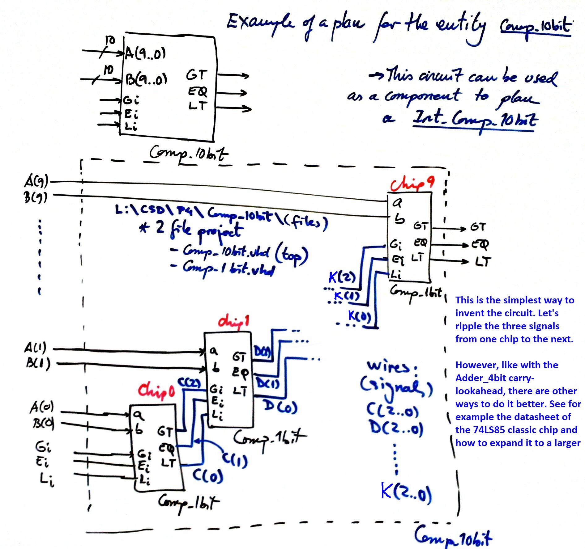
Project 2) Solve the Comp_12bit. Natural (whole) numbers in radix-2. This is an idea of a plan for N = 10.
Project 3) Solve the Int_comp_12bit for integers in 2C. This is an idea on how to deduce an algorithm and therefore the final plan for N = 8.
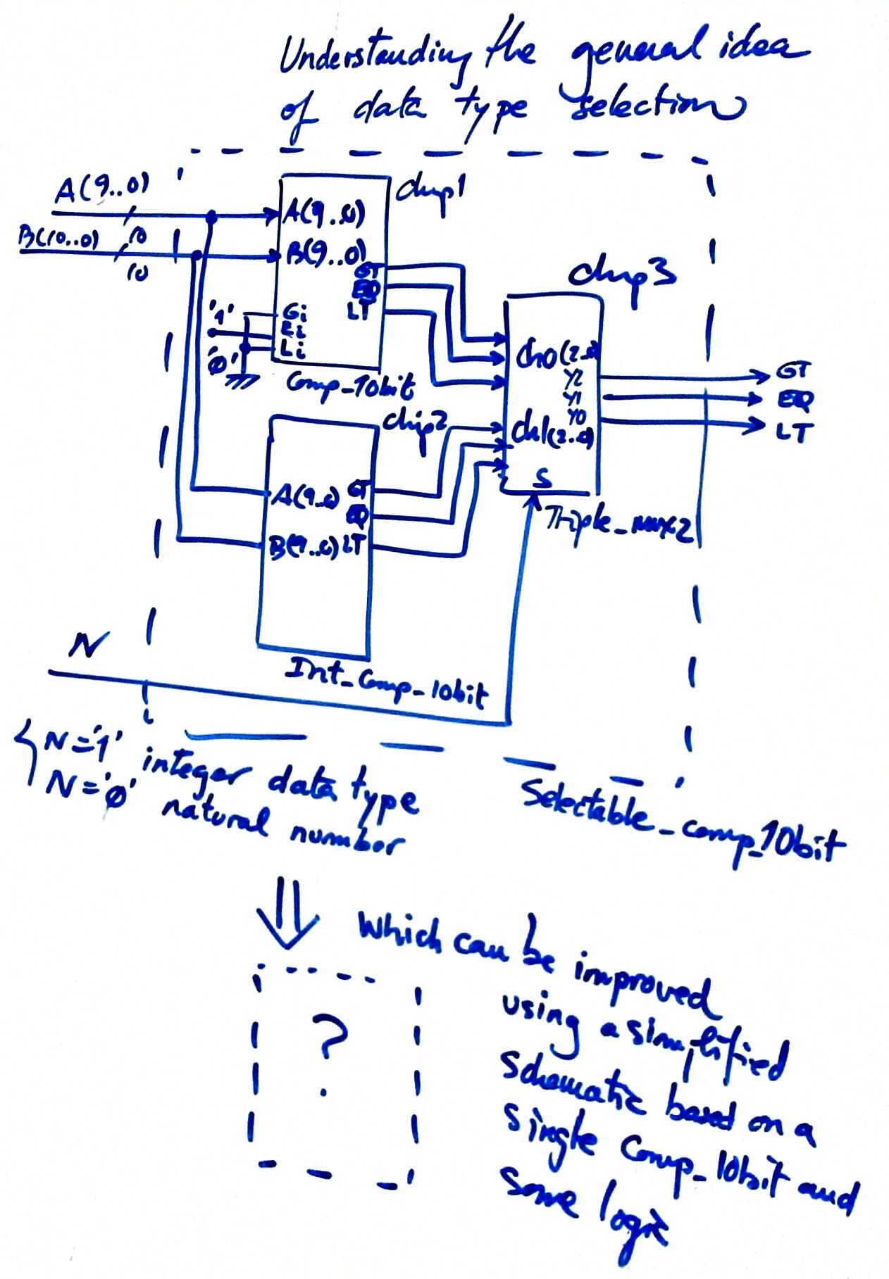
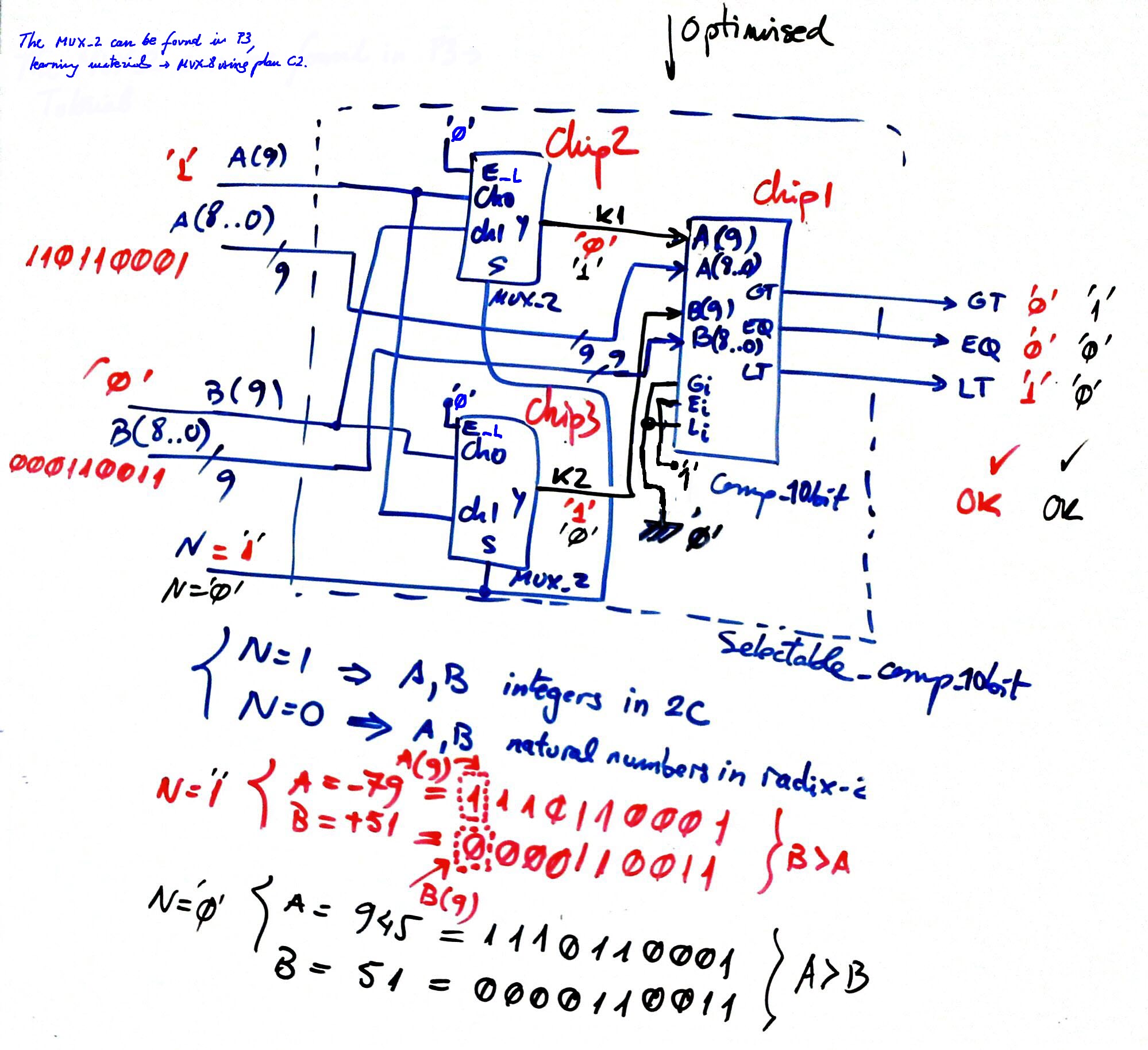
Project 4) Solve the Selectable_comp_12bit as in problem 4.3 which is for 10 bit comparisons. The input N decides which data type to compare: natural or integer numbers. This is the conceptual idea (10 bit) of a circuit for two data types. Ths is how the final plan (10 bit) may look like if only one Comp_12bit is desired for both, radix-2 numbers and signed integers?
For example, the adder and subtractor can be subdivided in:
Project 5) [Project F. Due date April 4]
|
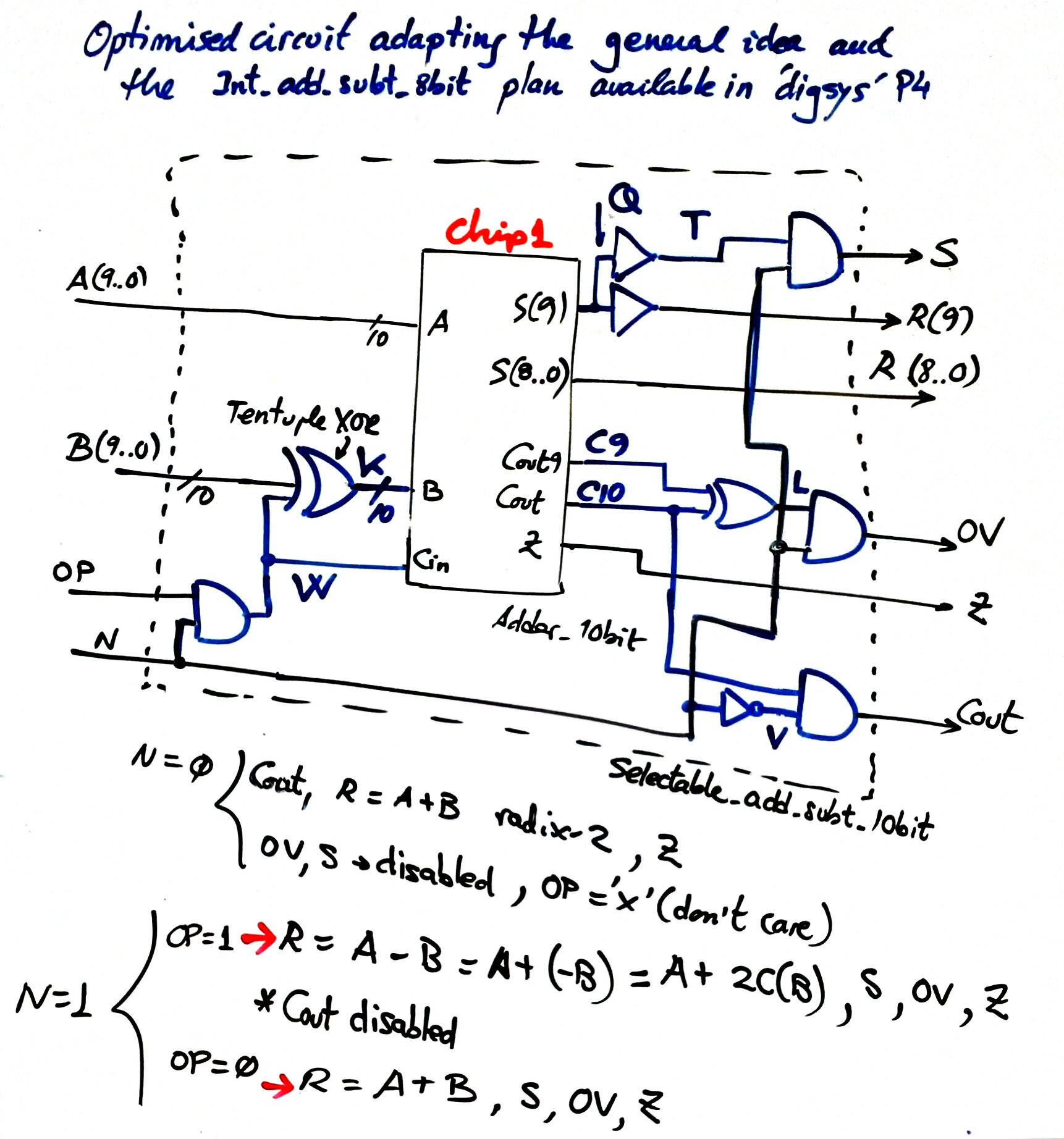
Project 6) Solve the project Selectable_add_subt_12bit. The input N decides which data type to add or subtract: natural or integer numbers. This is the conceptual idea and a possible plan. This is a video rec. on how to translate such plan into a VHDL equivalent file for developing the project.
Perhaps there is something to discuss about the Z flag in this Project 6. When using radix-2 numbers, Z includes the Cout; however, when working with integer numbers, Z doesn't have to include the Cout.
And, finally, as the Project 7, combine the selectable comparator (Project 4) and adder-subtractor (Project 6) in the entity represented in Fig.1, as another opportunity to pratice with plan C2:
Project 7) Solve the project Selectable_add_subt_comp_12bit. Which is the maximum speed of computing of this circuit when synthesised for a target FPGA Cyclone IV EP4CE115F29C7N?
|
Solving projects in cooperative groups is not easy, on the contrary. Thus, clarify which task each team mate has to do and is responsible of, in which time the task has to be done, and how are you assuring that everybody learns all the project sections. Discuss extensively the problem (specifications and plan) with your team mates and instructors using pen & paper and some numbers to test before starting the developing and verification using the EDA tools. Remember that the VHDL development and test cannot be graded unless there is a detailed original plan. This is a kind of a list of items that may be taken into consideration for (auto)assessment purposes, but it is also the same list that is useful for solving the project:
|
PLA#2.1 on 1-bit memory cells and FSM
Project G Design circuits using 1-bit memory cells. Due date April 24th.
The task A / B / C / D (pdf, docx) has two objectives: learning about latches and flip-flops and applying them in circuits such as problem 5.3 - 5.5 (synchronous) and 5.4 - 5.8 - 5.9 (asynchronous). Each team member has been assigned a given task. And this a Proteus circuit to play with flop-flops as if we were in the laboratory building such circuits for real using the classic 4000 CMOS series (when picking parts from the library to mount your circuit, do this initialization --> Tool--> global annotation --> total) . Another circuit that will help you to understand how to analyse an asynchronous circuit is the binary and one-hot counter presented in P5 as a tutorial.
NOTE 1: First of all, solve at least one of the five example problems form the CSD collection listed above.
NOTE 2: Take our role as a lecturer to be able to explain how to deduce the timing diagram and to explain it to all the students in class. Therefore, you need to prepare class notes, slides, diagrams, and a sequence of steps to make the problem comprehensible to other students.
NOTE 3: One way to tackle the problem solution, because most of the circuits have several CLK signals, may be:
1) Study a single flip-flop and deduce its timing diagram in paper.
2) Connect two flip-flops in a way that you have two CLK signals and try to deduce the timing diagram in paper. In this way, for example you can deduce that the Circuit C is not going to switch at all (rec.), and so, you can modify it in one way or another to make it run and generate waveforms);
3) Now, go for your complete circuit. Check your solution with Proteus results and VHDL. The Problem 5.9 has an extensive tutorial explaining such approach. This is a rec. on the solution of the Problem 5.4, the last part of which shows how to deduce the timing diagram in paper.
NOTE 4: Do not panic. Take it easy. This circuits are invented simply to show you how difficult, unpredictable and unreliable are the asynchronous circuits that you can think of simply connecting gates and FF in any way. Naturally, we have something better the next P6.
|
This is a kind of a list of items that may be taken into consideration for (auto)assessment purposes, but it is also the same list that is useful for solving the project: It is an analysis, so the plan is as indicated in the video rec.: Three different methods for obtaining the solution and being able to discuss the way the circuit works. 1. Paper analysis. 3p. Two or three analysis phases until the final circuit composed of four FF have to be included (this is the NOTE 3 above). And the text/pictures/graphics must be as indicated in NOTE 2. 2. Capturing the schematic in Proteus. 2p. Proteus files have to be included. Discussion about the waveforms, naturally. A simple capture means nothing. Which are the codes generated by the circuit so that you can compare with the other methods. 3. Analysing the project using VHDL. 3p. Quartus Prime and ModelSim projects have to be included to have a meaning. Discussion in handwriting on the waveforms. 4. Measuring how fast is the circuit for a MAX II CPLD. 2p. The timer analyser and the gate-level ModelSim projects has to be included and discussed in handwriting. Copied waveforms, schematics, etc. wil not be considered for grading, reports and projects must be individual, authentic and original. |
|
|
Project H FSM applications. Due date: April 30th
This is the Problem 6.5 in the CSD collection: designing a water tank controller. The project includes the section g on the method of ROM memory for implementing logic functions. In the tutorial there are two complete examples. Some ideas to start.
|
This is a kind of a list of items that may be taken into consideration for (auto)assessment purposes, but it is also the same list that is useful for solving the project:
Copied waveforms, schematics, etc. wil not be considered for grading, reports and projects must be individual, authentic and original. |
PLA#2.2 on FSM and dedicated processors
Project I Design a counter using Plan X. Due date: May 15.
Designing several types of counters taking the Problem 7.8 in the CSD collection as example and guidance. Plan C2 sections (g and h) will become theory to be discussed in paper in the end of the project. Those are the task A / B / C / D (pdf, docx) assigned for you individually. And, please, take advantage of the many comments feedbacked from previous projects, in a way that you try your best for not repeating the same kind of errors.
NOTE: First of all, read the project to be solved and draw an strategy. For instance, this is plan X, right?, therefore:
step 1) study and solve step by step the tutorial on the design of a Counter_BCD_1digit;
step 2) invent you counter and solve it to the end counting only up, which means that the UD_L control signal is not considered;
step 3) do it again introducing the UD_L signals discussing what has to be modified.
|
|
Project J Challenge: design a pulse generator as a dedicated processor architecture. Due date: delayed to May 31
This is the first draft of the project ( (rec.):
 |
| Fig. 1. Initial draft of the pulse generator circuit. |
This an example of assignment. (pdf, docx). The key idea is to invent the architecture of the dedicated processor capable of solving the project specifications. This is a rec. discussing the many components that may be included in the architecture.
So, what goes next now is the proposal of an architecture. How many components may it contain? How many states will the control unit have?
And so, Fig. 2 and Fig. 3 are a kind of spoiler: an example of proposed architecture magining how the datapath can be designed, and then following with the top entity rec. The CLK_generator (Chip3), the debouncing_filter (chip5) and the RS_FF (or JK_FF) (Chip4) can be found in the corresponding previous projects. And the same for the internal components in the datapath: Counter_mod16, shift_reg_4bit, and data_reg_4bit can be used as models to copy and adapt for the Counter_mod_1048576 (Chip5), shift_reg_16bit (Chip1) and the Data_reg_19bit (Chip2).
 |
Fig. 2. Example of datapath with enough operational resources for processing the information in this application (click the picture to zoom) |
 |
Fig. 3. Example of top entity internal architecture (click to zoom). |
Perhaps it is a good time to discuss why to use a debouncing filter to interface a key, and how to connect it to the RS_FF for saving the click pulse until the control unit acknowledges it. Fig. 4 represents typical waveforms in this tricky circuit working synchronously with two CLK signals: a low frequency signal for the physical phenomena of detecting key clicks, and a high frequency CLK for running the dedicated processor. Rec.
 |
Fig. 4. Time diagram analysis of the debouncing filter and the 1-bit memory cell. |
Therefore, from now on, what is left is the state diagram for the Control_unit (Chip2). Can you invent it?
Fig. 5 is another spoiler for the control unit state diagram. The key idea to invent this type of diagrams is to visualise examining the timing diagram how many different actions must be taken. And this is only the initial state diagram to start the development process, because at this level of complexity, development and simulation tools play a fundamental role to debug errors, add modifications and be able to finalise the project.
 |
| Fig. 5. Example of state diagram. |
This application is an example of advanced circuit on the possibilities of hardware design. Many concepts and circuits here will keep the meaning at the end of Chapter 3 where we'll have the opportunity to build them again but using a microcontroller as an alternative design technology.
The way to assess this project is: paper work from 1 to 7 ---> 7p and then, 8-9-10 development and testing of (some circuits) --> 3p.
Completing all the Pulse_generator circuit perhaps is too much, something that you can finish once the course ended if you wish and have interest in this subject. This is also one of the learning outcomes of CSD, design time accounting. How much a real application design may cost in engineer's time (and thus in money)?
| NOTE: Do not solve the complete project, you don't have time now within the course constraints. As indicated above, the project is for you to explain from 1 to 7 the circuit as it is specified and planned in the pictures above. It is intented as a kind of preparation for the final P_Ch3. Then, if you like to mark 8-9-10, simply take one or two components to develop and test. |
PLA#3.1 on microcontroller circuits
Project K Design a combinational circuit using the PIC18F4520. Due date: June 5. Delayed to June 7, 22:00.
This is a training project for comprehending how to connect pins and how to organise the program. Similar to the Lab9 Dual_MUX_4 tutorial and the P9 project.
Specifications: truth table, symbol, timing diagram. Planning: 1) schematic, 2) program organisation, hardware-software diagram, functions ad flowcharts. Development: MPLABX project and compilation. Testing: Proteus simulation.
Follow the usual design flow but this time programing only a few statements and running the test, and then another few sentences and run again the testing, and so on. For example in the circuit A, read only the input Ei and verify in a watch window that the variable var_Ei is correct reading the signal's logic values. Only when this signal is polled correctly it is possible to continue capturing the D(7..0) vector step by step (port by port).
And this is a rec. on how to start a new project from the Dual_MUX4 tutorial following the step by step strategy (one line of code at a time).
 |
| Fig. 1. Four different combinational circuits from Chapter 1 used again to discover how to configure microcontroller digital inputs and outputs and how to organise the software section of the application. |
Find all the details and task assigments in Atenea Project K.
|
|
Project L Designing a FSM using using the PIC18F4520. Due date: June 9, from 8:35 to 9:55.
Organised as a synchronous individual class activity with submission of documents online. Find all the details of the task at Atenea Project L.
Final P_Ch3, report + oral presentation
Individual for the next new due date: Tuesday June 30, 13:00.
P_Ch3: Each student has a project assigned. Find all the details of the task at Atenea P_Ch3 oral presentation and report.
Other similar projects from former courses
1920Q1. This page shows PLA project assigments.
| Home Term 23/24-Q2 Contact Products Electronic devices and companies Software Books Magazines Instruments DEE Library EETAC DEEL |

|
|
| Web activa des de 09/2001, @ F. J. Robert, J. Jordana. Web editat amb Microsoft Expression Web 4. El contingut és un complement als materials d'estudi del curs Circuits i Sistemes Digitals disponibles al campus digital Atenea. Llicència:Reconeixement 4.0 Internacional de Creative Commons |