|
|
Bachelor's Degree in Telecommunications Systems and in Network Engineering |
|
|
|
||
|
|
Comp_1bit plan B: behavioural single-file VHDL |
|
|
|
||
Design of a 1-bit expandable comparator (Plan B)
1. Specifications
Design a 1-bit expandable comparator Comb_1bit using a single file based on a behavioural interpretation of the circuit's truth table, plan B.
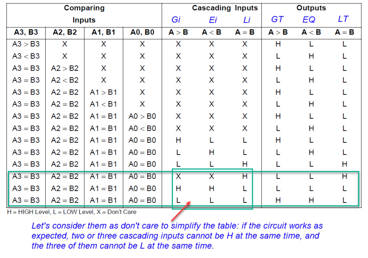
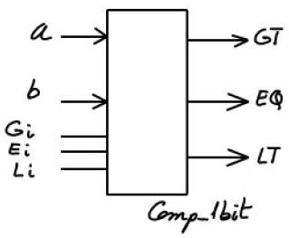
It has the symbol and truth table represented in Fig. 1. The truth table has been adapted from the standard 4-bit commercial comparator chip 74LS85, the datasheet of which can be used to figure out how to chain comparator components to obtain larger circuits of the same kind.
 |
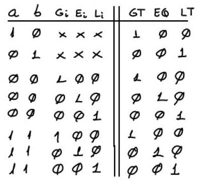 |
Fig. 1. Symbol and truth table of a 1-bit comparator with extra signals for expandability. |
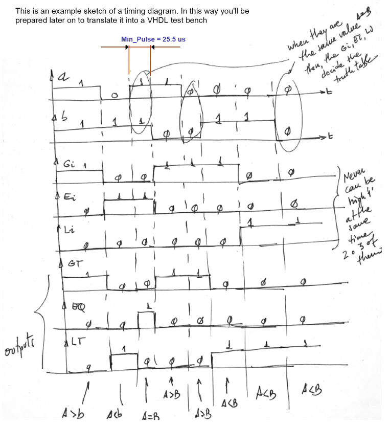
In Fig. 2 there is a simple sketch that represents some values of the truth table in time. The timing diagram wll be used in section 4th for testing the circuit using a VHDL testbench. All the 32 combinations can be applied sequentially in time to complete the test.
|
| Fig. 2. Timing diagram where all the inputs are applied sequentially and hence, the output is predicted accordingly to the truth table. |
2. Planning
The VHDL file will be named Comp_1bit.vhd and the project name and location will be: Comp_1bit_prj, "L:\CSD\P3\Comp_1bit_B\(files...) "
Plan B schematic to be translated to VHDL.
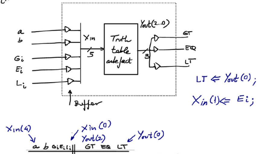 |
| Fig. 3. Schematic where the truth table is used as an artefact along with some buffers to interface ports. |
3. Developing the project using EDA tools
Plan B behavioural file from schematic above Comp_1bit.vhd
Run a EDA project to synthesise the circuit. Fig. 3 shows an example of RTL schematic.
 |
Fig. 3. RTL view. The EDA synthesiser has interpreted the circuit in this way. |
Print and examine the technology view as well. Compare it with other realisations accordingly to plan A or plan C2. Is there any difference to highlight?
4. Testing and validating the design
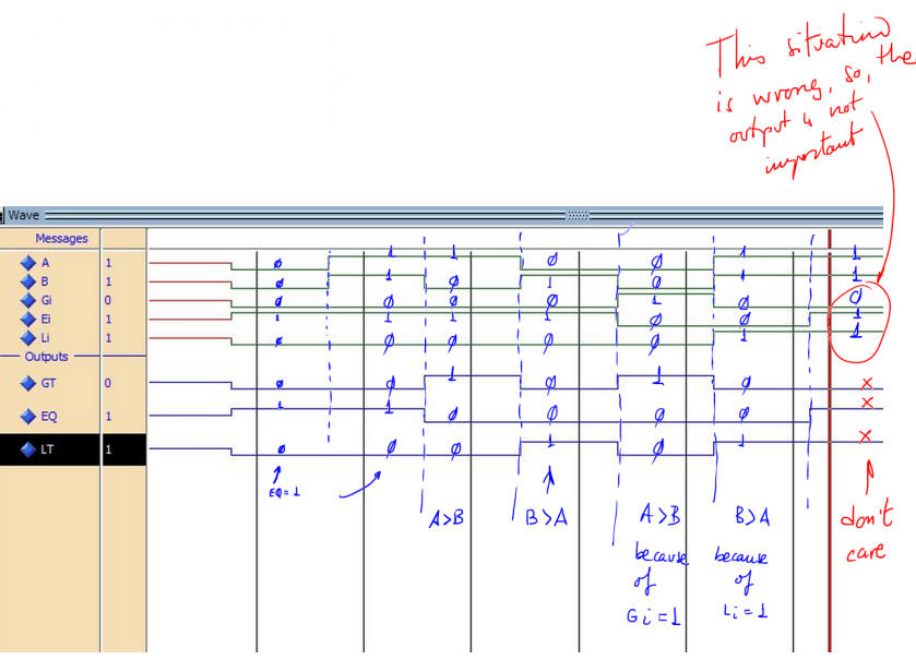
An example test bench Comp_1bit_tb.vhd. Run the VHDL simulation EDA tool to obtain and discuss the timing diagram. Remember that from the testing point of view, even if you have designed the Adder_1bit using several plans, you can use all the time the same testbench.
 |
|
Fig. 4. Example testbench showing results. |
5. Report
Project report starting with the template sheets of paper, scanned figures, file listings, docx , pptx, or any other resources.
6. Prototyping
Use training boards and perform laboratory measurements to verify how the circuit works.
| Home Term 26/27-Q1 Contact Products Electronic devices and companies Software Books Magazines Instruments DEE Library EETAC DEEL |

|
|
| Web activa des de 09/2001, @ F. J. Robert, Web editat amb Microsoft Expression Web 4. El contingut és un complement als materials d'estudi del curs Circuits i Sistemes Digitals disponibles al campus digital Atenea. Llicència:Reconeixement 4.0 Internacional de Creative Commons |