|
|
Bachelor's Degree in Telecommunications Systems and in Network Engineering |
|
|
|
1-digit BCD counter plan X |
Solving FSM in C (state enumeration)
| 1. Specifications | Planning | Dev. & test | Prototype | report |
To demonstrate how a sequential circuit can be implemented using a microcontroller for instance in a target chip PIC18F46K22 and the latest Microchip MPLAB X IDE and XC8 tools, let us implement some features of a typical 1-digit BCD counter type 74HCT160 or 74HCT190. Full rec.
|
|
Fig. 1. Internal structure of the classic counter chip 74HCT160 to be implemented using a μC. Note: As you see, we fix LD_L = '1', thus, chip's parallel load functionality is always disabled. Synchronous parallel load may be proposed as another plan Y application. |

The chip and features to be implemented can be readapted as represented in Fig. 2 using our naming conventions as in Counter_BCD_1digit example on plan X.
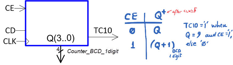  |
| Fig. 2. Symbol (Visio) and its function table as studied in Chapter 2. Some initial hardware details on how to connect inputs and outputs to demonstrate the counter. |
Propose a timing diagram as in Fig. 3 and adapt it to use RAM variables. Thus, a question arises immediately: how to make the microcontroller sensitive to CLK signal edges? Is it the same that reading inputs (polling) in the main program or we have to find a way to detect signal edges? What is the difference between this external CLK that runs the counter application and the quartz oscillator OSC at 8 MHz that runs the microcomputer?
 |
|
Fig. 3. Example of timing diagram for the initial design phase #1. Signals will be converted in to RAM variables. |
Switches will be read using polling in read_inputs(), as proposed in P9. Push-button actions (pressing or realising) or equivalently, signal transitions or active edges will be detected using the key concept of interrupt.
| Specifications | 2. Planning | Dev. & test | Prototype | report |
The project design flow when using microcontroller technology is depicted in Fig. 4.
 |
|
Fig. 4. Design flow for developing and testing a single design step at a time. |
Therefore, as most of our proposed projects in this Chapter 3, the design of the Counter_BCD_1digit, will be organised in several phases and steps. This LAB10 tutorial covers only the first step #1 of the design phase #1.
- Design phase #1: Basic counter.
- Step #1: Design the basic up counter with TC10 and CE.
- Step #2: Add reversibility (UD_L)
Project location:
C:\CSD\P10\Counter_BCD_1digit\(files)
- Design phase #2: Counter with LCD. Solved as a complete tutorial at: Counter_BCD_1digit_LCD
- Step #1: Display only static text messages, the "Hello World" for testing hardware and software.
- Step #2: Display dynamic data such the state numbers.
- Design phase #3: Using internal timers to replace the external CLK. Solved as a complete tutorial at: Counter_BCD_1digit_LCD_TMR0
- Step #1: TMR0
- Step #2: TMR2
What is time resolution, accuracy, precision, reliability? Which timer is more accurate? Which is the key component for high resolution timing?
Note: enumerating states is perfect for designing FSM. As you see, we also propose state enumeration Plan X for implementing counters. However, it has its limitations when the counter has many states or many state transitions. Therefore, as we did in P7 for large counters, we will study how plan Y is adapted to µC in the second tutorial of this laboratory Counter_mod1572. Besides, other features such parallel load (LD and Din) are easily implemented when var_current_state is encoded as a number in binary sequential (radix-2).
Design phase #1. Step #1: Design a basic up counter with TC10 and CE. For instance as it was done in Counter_BCD_1digit.
Draw the state diagram as in Fig. 5. Note that in this chapter we use memory variables to solve the diagram. External signals such pin CE will be polled in read_inputs() so that var_CE will contain its value. CLK active edge will be detected using the external interrupt INT0. In this application, all state transitions happens only when var_CLK_flag is set. Output variables such var_BCD_code, represented as always in parenthesis and using another colour, are written to the corresponding microcontroller pins.
 |
Fig. 5. State diagram driven by interrupts on external edge detection. |
Let us repeat this substantial concept: be aware of the difference between a level-sensitive signal such CE (read/poll) from a switch, and an edge-sensitive signal (interrupt) from a push-button, because they are interfaced using specific mechanisms. The nature of such signals will be highlighted in the naming convention of RAM variables: an edge-sensitive signal like CLK will be named var_CLK_flag, while a level-sensitive input such CE will be named simply var_CE.
A) Planning hardware
We can use any pin from any µC port to connect inputs and outputs. However, we have to pay attention to connect external interrupt sources such CLK, for not all the pins have the required interrupt logic. The target chip PIC18F46K22 features only three pins for interfacing external interrupts: RB0/INT0, RB1/INT1 or RB2/INT2.
 |
Fig. 6a. Only RB0, RB1 and RB2 port pins have INT logic to detect signal edges. |
Circuit and port connections are represented in Fig. 6b. If the system has to be prototyped in a later design stage on a training board such CSD_PICstick, PICDEM2 PLUS or EXPLORER 8, we can use the board connectors to attach input and output components such switches, resistors, LED, etc. Or instead, we can use the boards resources when available. CSD_PICstick contains up to 9 LED, one switch and one push-button, enough for this application.
 |
Fig. 6b. Hardware used in this application
adapted to the CSD_PICstick. The idea is to
connect the CLK signal to an external interrupt pin (INT0).
We can select which edge, falling or rising, is going to
trigger the interrupt flag (INT0IF = 1).
|
B) Planning software
The general idea for solving the FSM architecture is represented in Fig. 7a. The concepts of CC1 and CC2 combinational circuits inherited from Chapter 2 are the same. However, this time, we will implement these truth tables using software routines and input and output RAM variables. The state register and the next_state signal is not required because we simply use a RAM variable like var_curent_state to encode state labels. The next state value will be asserted after executing again the state_logic function located in the infinite loop.
The CLK synchronisation mechanism is different from Chapter 2. The FSM function state_logic() will be executed only when there is a CLK edge detection (var_CLK_flag = 1) by means of the external interrupt mechanism.
a) |
 |
b) |
 |
Fig. 7. The FSM adaptation and the software organisation used in this application. |
|
This special C code organisation allows you to take full advantage of previous Chapter 1 and 2. Almost all the content learnt since now can be fully applied here again when we switch to programming microcontrollers instead of describing hardware. Furthermore, even if we choose other microcontrollers such Arduino or microcomputers like Raspberry Pi or any other similar platform, the main ideas and adaptations remain the same. There is a huge advantage organising as separate and independent pieces of software the hardware-dependent functions such read_inputs or write_outputs acting as hardware drivers.
In Fig. 8 there is an example of software-hardware diagram. Another advantage of this organisation is that software functions output_logic() and state_logic() are completely compatible among platforms and programming languages. Only hardware-dependent functions (drivers) have to be rewritten when changing microcontrollers or programming environments.
 |
|
Fig. 8. Hardware-software diagram. Hardware interface functions are drawn in black and software functions based on RAM memory in blue. The picture also shows the circuit and the associated configuration bits for allowing the external interrupt INT0 to detect CLK's falling or rising edges (this feature is configurable). |
All the main RAM variables to handle the FSM are represented in Fig. 9. All the variables are kept char type (uint8_t) for being able to watch them easily in our simulation and debugging tool.
 |
|
Fig. 9. RAM variables list. |
Draw the main ideas of init_system(). Configure input and output pins as indicated in Fig. 10.
 |
|
Fig. 10. TRIS configuration bits. |
Infer as shown in Fig. 11a how to organise the interrupt service routine ISR() to handle CLK's falling edge detections. Consider as well interrupt configuration bits to enable INT0. Configure the INT0 active edge for triggering interrupts as shown in Fig. 11b.
Notice how organising the software in this very specific set of functions, each one with a very well defined objective, it is easy to work in group with several team members working concurrently in different functions of the same project.
 |
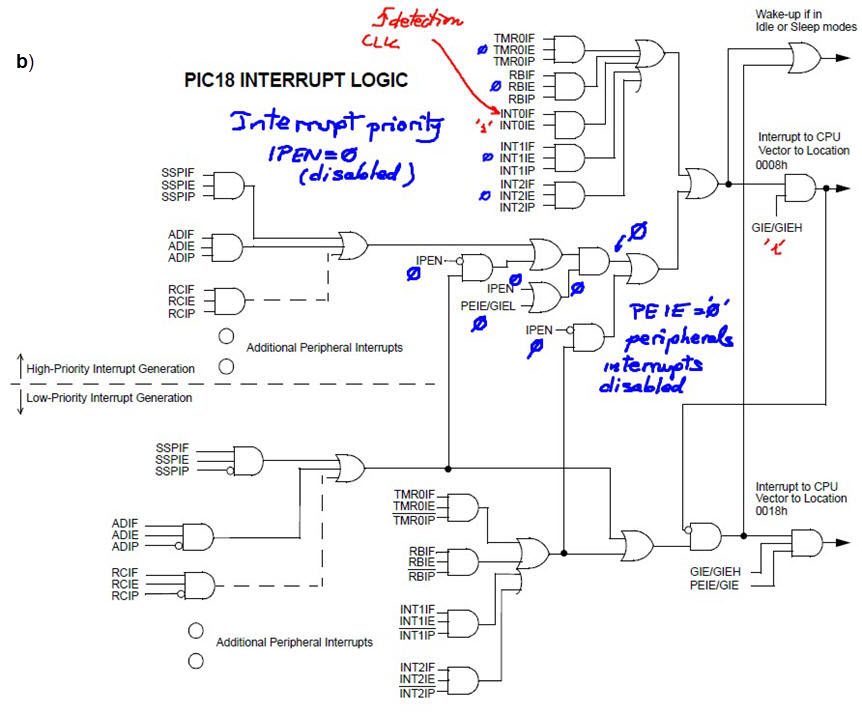
Fig. 11. a)Interrupt service routine for setting var_CLK_flag. This key function is for synchronising the execution of the FSM on active CLK edges.
b) The interrupt logic to enable or disable each interrupt source.
|
 |
|
And now, it is necessary to discuss how to transfer all the state transitions into a truth table (the CC1).
Draw state_logic() truth table.
 |
|
| Fig. 12. Truth table for state_logic() function. When the input var_CLK_flag is used for all transitions there is no need to add it to the truth table (As we did with the CLK signal in Chapter II projects). | |
Translate it into a behavioural flowchart. All transitions are affected by the CLK edge detection interrupt as expected in counters. The function read_inputs() executed before state_logic() captures the pins of interest and generates their corresponding RAM variables.
 |
Fig. 13. Translating state_logic() truth table into a behavioural flowchart as we did in VHDL plan B. In this way the C statements can be easily imagined. |
Finally, what is left to finish this project planning is the same idea but for the outputs, how to translate all the outputs in parenthesis into a truth able and its equivalent flowchart?
Draw the output_logic() truth table.
 |
|
| Fig. 14. Truth table for output_logic() function. | |
Translate the truth table into a behavioural plan B flowchart in the same way we did in VHDL.
 |
Fig. 15. Translating output_logic() truth table into a behavioural flowchart so that C statements can be easily imagined. |
Draw the flowchart of read_inputs(). Basic function to poll input voltages as in L9.3. Translate the flowchart into C using bitwise operations.
Draw the flowchart of write_outputs(). Basic function to write pins voltages as in L9.4. Translate the flowchart into C using bitwise operations.
Notice how organising the software in this very specific set of functions, each one with a very well defined objective, it is easy to work in group with several team members working concurrently in different functions of the same project.
Additional questions:
- How long does it take to execute the code and thus which is the reading/polling speed?
- How many RAM bytes are used in this application?
- Which configuration bits has to be programmed to setup interruptions from INT0?
- How to program the INT0 active edge (rising or falling)?
- How many external interrupt sources INT has the microcontroller that you can choose from?
|
|
Important remarks: Do NOT write the C code without having discussed on a sheet of paper your planning and flowcharts. Therefore, four or five sheets of paper are expected to clarify and organise every aspect of hardware and software. Reuse materials from previous projects. Do NOT copy and paste digsys pictures into your reports, but analyse and redraw them in your own way. It is the only way to grasp full details and be able to ask meaningful questions to comprehend projects.
|
|
Step #2: Enhance the previous circuit adding the UD_L feature. Only when step #1 is fully develop and debugged using step by step execution and watching variables of interest.
|
|
(Optional) Step #3: Add the parallel load (LD), which means changing completely from plan X to plan Y. Additionally, some actions has to be considered when an invalid data is inputted by the user (D = 1010, 1011, ... 1111) to prevent unexpected states, for instance, reset the system to build a safe FSM. Therefore, it is better to solve this step #3 after studying the next tutorial below on plan Y.
| Specifications | Planning | 3. Dev. & 4. test | Prototype | report |
A) Developing hardware
This is an example of circuit schematic "Counter_BCD_1digit.pdsprj". This capture is easily generated copying and adapting a similar example.
 |
Fig. 16. Hardware connections to solve step #1 of this project. A switch allows you to select the CLK source: single pulses from a push-button or an external oscillator. |
B) Developing software
The C source file "Counter_BCD_1digit.c" for step #1 where only count enable and up counting are developed. Add the "config.h" header to your project to fix the mC configuration bits.
Run the IDE and start a new project in the corresponding folder. Name it as usual: Counter_BCD_1digit_prj.
Compile and generate the "*.cof" (includes symbolic information for debugging) and the "*.hex" (to download to the microcontroller) output configuration files.
Check the number of resources used: the size of the program, the number of memory bytes (RAM).
C) Step-by-step testing
Run Proteus and test the circuit using step by step, break points and the watch window tools. Remember that the key strategy is to write a few lines of code at a time, compile, run and test. And only when it works, add some more code after having transferred truth tables and algorithms into flowcharts.
 |
| Fig. 17. Example capture from Proteus running the application setting 20 Hz as the CLK frequency. |
Questions:
- How long does it take to run the main loop?
- How long does it take to execute an interrupt? and therefore, what is the maximum CLK frequency you should apply in order to make it run correctly?
- How can you compare these magnitudes with values attained in chapter II designing hardware counters in VHDL for target FPGA or CPLD?
 |
 |
| Fig. 18. a) Example capture from Proteus logic analyser instrument screen and the analysis to determine whether the circuit works correctly (CE = 1). b) Printing the logic analyser screen for the project report requires changing colour configuration using white background to save printer ink and generate clear documentation. |
This is the compiled "Counter_BCD_1digit.zip" project.
| Specifications | Planning | Dev. & Test | 5. Prototype | Report |
Board CSD_PICstick. Target microcontroller: PIC18F46K22. Tools: MPLAB X + XC8 + Proteus MPLAB SNAP in-circuit debugger/programmer. Instruments: VB8012.
Experiment #1: Run the application and visualise results using the board resources. This is for checking the installation of the tools and programming environment.
Select the options and project properties.
 |
Fig. 19. Options for generating the executable files "*.hex" and "*elf". The MPLAB SNAP programmmer and debugger is selected as the current target tool. |
NOTE: Be aware on how the MPLAB SNAP is connected to the board's ICSP female connector as shown in Fig, 20 aligning pin 1 with the triangle indicator.
 |
Fig. 20. Plug the MPLAB SNAP to the CSD_PICstick board using the ICSP 6-pin connector. The triangle mark is the pin 1. |
Two applications can be used for programming the board once the "*.hex" file is generated, the icon embedded in the MPLABX IDE, as indicated in Fig. 21, or the application MPLAB IPE in Fig. 22 devoted to programming devices.
 |
Fig. 21. Programming the chip using the MPLAB X top tap "Make and Program Device Main project". |
 |
Fig. 22. Programming the chip using the MPLAB IPE |
Download and program the target chip "Counter_BCD_1digit_prj.X.production.hex". Play and verify that it works as expected and in the same way it did in the simulator.
If you keep the SNAP tool connected, you must click "Release from Reset" to regain control of the board from the in-circuit programmer.
 |
Fig. 23. Release from Reset. |
 |
Fig. 24. Board running the Counter_BCD_1digit. The full application "Counter_BCD_1digit.zip" |
Experiment #2 (optional): Download and program the target chip (*.elf) to use the in-circuit debugger. Watch RAM variables in MPLABX IDE. Add breakpoints and follow the program execution as we did in Proteus simulations.
  |
Fig. 25. Using the debugger embedded in MPLABX IDE. |
Experiment #3: Drive and visualise signals using the VB8012 instrument and its WaveForms app.
The VB8012 waveforms generator Wavegen is used to drive the CLK (RB0/INT0) signal using a BNC-banana cable, instead of clicking the board's push-button PB1 manually. Outputs can be visualised using logic analyser channels. Signals may be grouped into busses (vectors). The expansion header represented in Fig. 26a is very convenient for starting to connect instrument probes.
 |
Fig. 26a. 40-pin expansion male socket accessing all the µC pins and the signals of interest. |
Let us wire the circuit in three steps after the sketch in Fig. 26b.
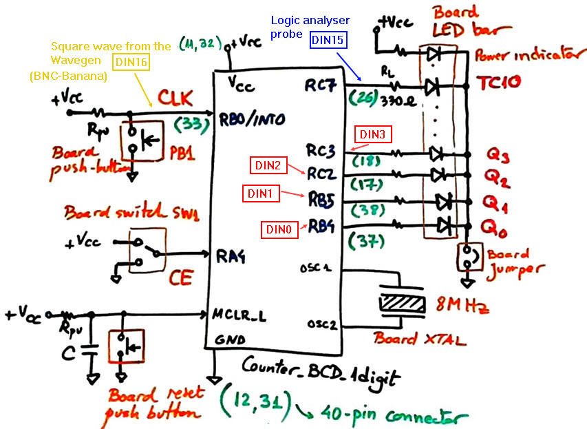 |
Fig. 26b. Attention: Draw this schematic in a sheet of paper before prototyping to be aware of the port pins, power supply, inputs and outputs used, and the instrument probes. |
Option #1: Connect instrument probes through the flat cable and the breadboard adapter.
In a first step, as shown in Fig. 27, we connect GND and VCC. We also duplicate in the protoboard the signal TC10 that is the LED7 in the CSD_PICstick at RC7 (pin 26), a kind of a monitor signal to check that the protoboard is powered correctly.
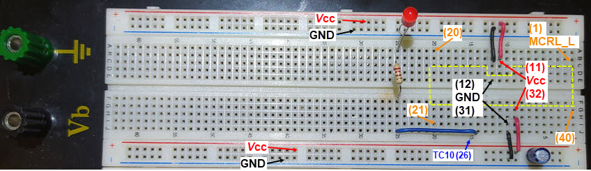 |
Fig. 27. Protoboard short connections to power rails. Use pliers or stripper to cut the wire insulation. We use a an electrolytic capacitor as a buffer for energy storage; be aware of its polarity. The upper-right number 1 hole will be the pin 1 of the adapter (see the yellow dotted shape). |
Now we have to verify that these simple connections are right and the breadboard is correctly powered. When experimenting in the laboratory, it is crucial to put all your senses in the circuit to avoid short-circuits and other costly hazards. Attach the 40-pin flat cable adapter and connect the CSD_PICstick to run the experiment. The duplicated TC10 LED has to light correctly when at state9 and CE = '1'. Remember that the count enable signal is the CSD_PICstick switch SW1.
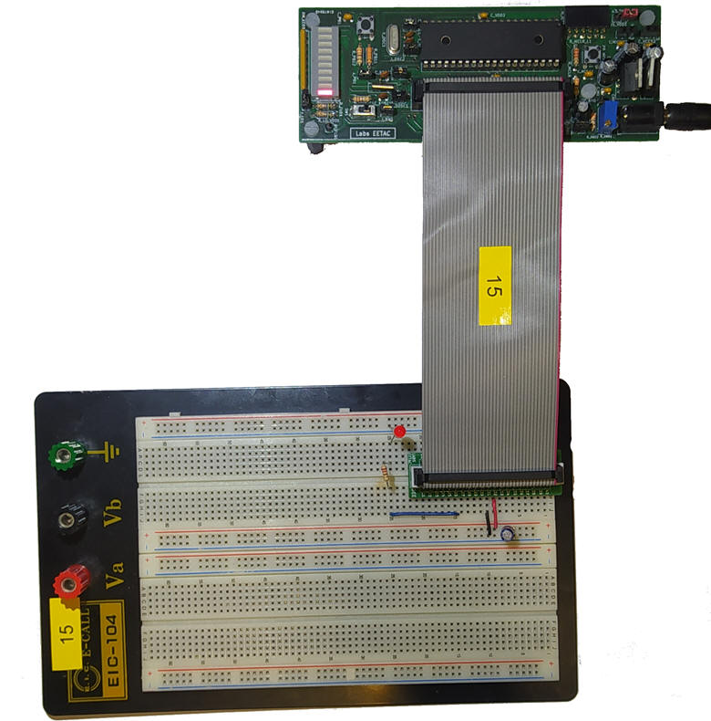 |
Fig. 28. Running the experiment #1 with the 40-pin cable adapter attached to the protoboard. |
When this first step works correctly, switch off the CSD_PICstick DC power adapter and unplug the cable adapter, to continue.
In a second step, as shown in Fig. 29, we use 20 cm male-male coloured flexible wires for facilitating the connections to the logic analyser probes and the Wavegen signal generator that will replace the CLK push-button generating a train of pulses.
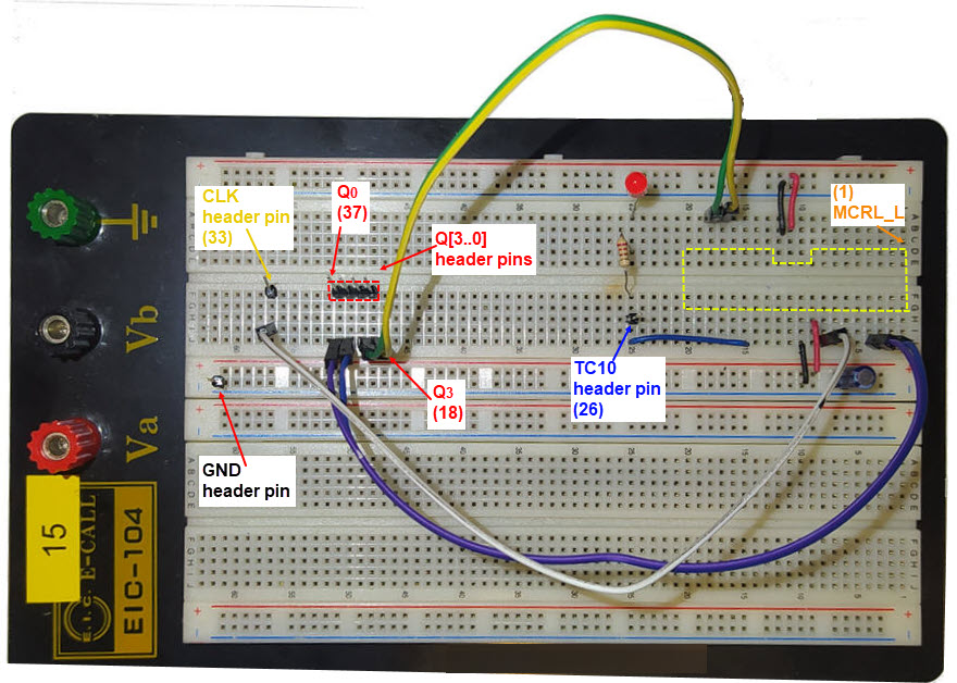 |
Fig. 29. Flexible wires to connect the male headers for the instrument probes. |
In a third step, as shown in Fig. 30, we can complete the setup connecting the instrument probes to the male header pins and the power supply adapter to switch on and run the application.
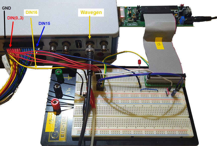 |
Fig. 30. The final circuit for measuring signals and experimenting. |
Using a BNC-banana cable, let us connect the Wavegen from the compact instrument VB8012 to drive the external CLK signal.
Let us use the logic analyser probes and long 20 mm male header pins to visualise the counter signals. This is the instrument setup file "VB8012_setup_Counter_BCD_1digit.dwf3work".
Modify the CLK frequency and start experimenting.
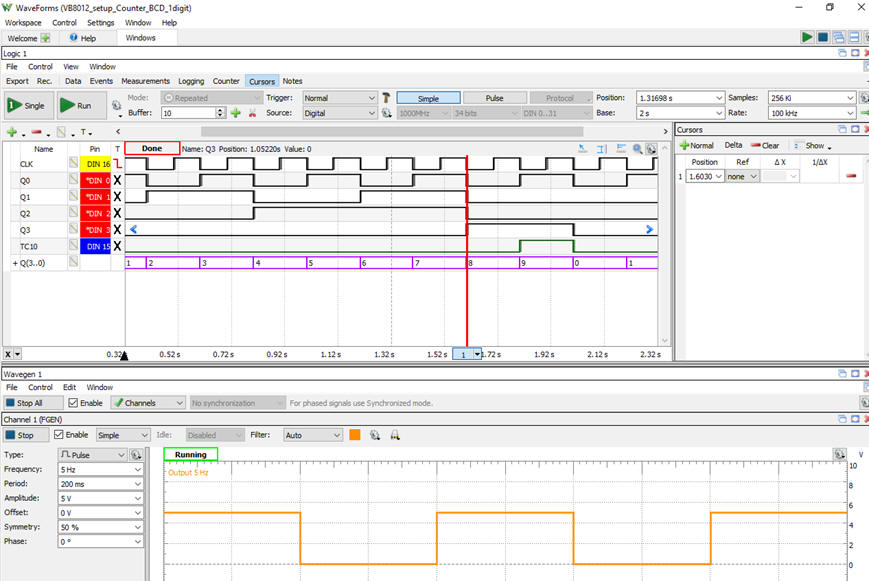 |
Fig. 31. Measured waveforms using the VB8012 compact instrument. |
Measure the propagation time from CLK to output as represented in Fig. 32. Why the output signals are not set at the same time? Why we can observe illegal codes for some state transitions?
 |
Fig. 32. Zooming on a given CLK falling edge event allows measuring the propagation time from CLK to output (tCO). |
Which may be the maximum CLK frequency? Which is the relation of such frequency with the target board's crystal oscillator?
Option #2: Alternatively, for this simple experiment, we can connect instrument probes directly to the CSD_PICstick 40-pin expansion male socket.
No need to use the protoboard for this experiment, the instrument probes are attached to the 40-pin socket male pins.
 |
| Fig. 33. 40-pin expansion male socket used for direct probe connections to the logic analyser probes. |
| Specifications | Planning | Dev. & Test | Prototype | 6. Report |
Follow this rubric for writing reports.
| Home Term 26/27-Q1 Contact Products Electronic devices and companies Software Books Magazines Instruments DEE Library EETAC DEEL |

|
|
| Web activa des de 09/2001, @ F. J. Robert, Web editat amb Microsoft Expression Web 4. El contingut és un complement als materials d'estudi del curs Circuits i Sistemes Digitals disponibles al campus digital Atenea. Llicència:Reconeixement 4.0 Internacional de Creative Commons |