|
|
Bachelor's Degree in Telecommunications Systems and in Network Engineering |
|
|
|
||
|
|
Serial asynchronous receiver and transmitter (USART) |
|
|
|
||
Implement a universal serial asynchronous receiver and transmitter peripheral (USART) to establish a full-duplex between microcontrollers.
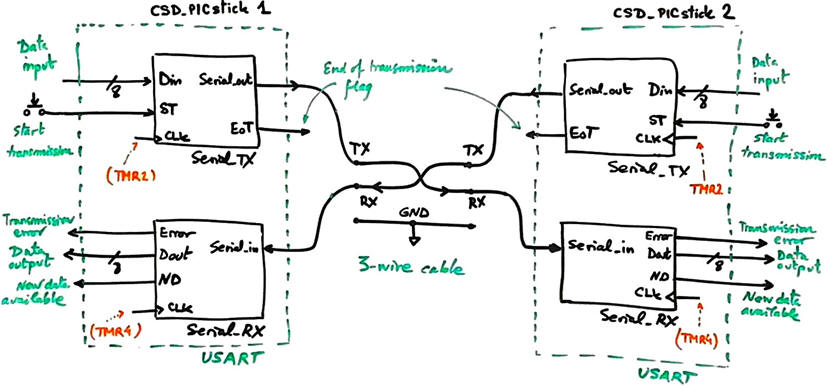 |
| Fig 1. The idea of the full-duplex serial communication experiment. |
A similar USART circuit is implemented as an VHDL application targeting an FPGA.
Design phase #1: Basic serial full-duplex communication using CSD bare-metal register-level programming styles and conventions prototyped on CSD_PICstick boards. This application will become another example of FSM for controlling the program execution.
The general organisation for this project will be divided in three steps. Firstly, we will modify and adapt to the CSD_PICstick the Serial_TX presented as the sequence of highlighted projects in P10-P11-P12 (phase #4 Serial_TX_LCD_TMR2). Secondly, we will implement the dual Serial_RX module; and finally, we will run both units from the main loop.
- Step #1 Serialise Din captured from switches.
- Step #2 Serial receiver to visualise Din in the LED bar.
- Step #3 Combined full-duplex serial communication using two CSD_PICstick boards.
Design phase #2: (advanced). The next design phase for this demonstration project is to abstract all the hardware. Let us reprogram the application using the professional tool MPLAB Code Configurator (MCC) Melody to interface the PIC18F enhanced universal synchronous/asynchronous receiver/transmitter (EUSART) peripheral as proposed in DEE Lab 11.
| 1. Specifications | Planning | Dev. & test | Prototype | Report |
Step #1 Implement the Serial_TX . Serialise Din captured from switches. Let us fix the following features that in a second phase can be made configurable: 8-bit data, parity odd, one stop bit, selectable transmission speed: 9.6 kb/s or 150 b/s. TMR2 will be used to generate interrupts every transmission period TP = TCLK.
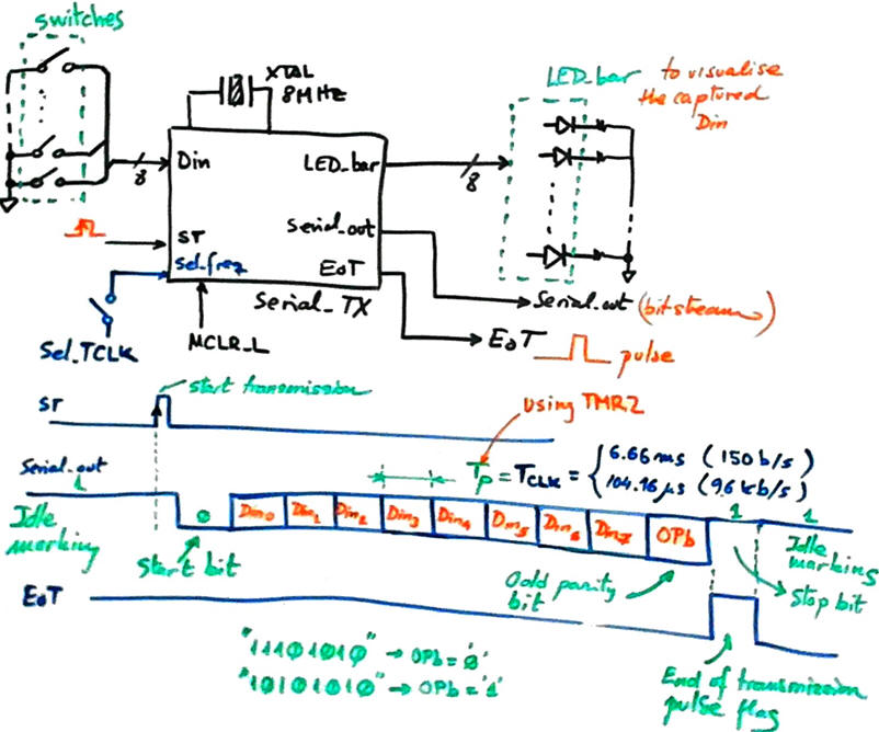 |
| Fig 2. Serial_TX symbol and transmission waveform. |
| Specifications | 2. Planning | Dev. & test | Prototype | Report |
A) Planning hardware
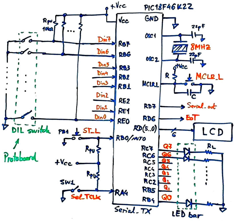
We will add switches to unused CSD_PICstick pins to input Din bytes. And we will use the LED bar to represent this information.
 |
|
Fig. 3. Transmitter hardware. |
B) Planning software
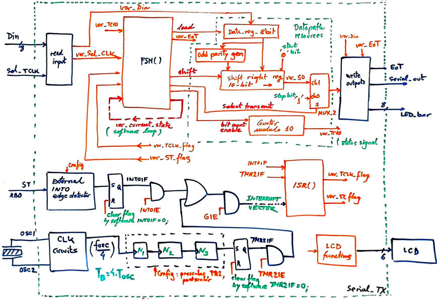
We can discuss which operational resources will be required to process the transmission frame. As represented in Fig. 4.
 |
|
Fig. 4. Hardware-software diagram required to organise the transmitter. |
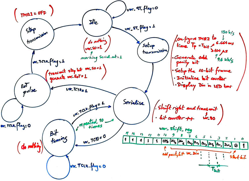
The FSM will be in charge of controlling the transmission of the serial frame once the start transmission signal is received.
 |
|
Fig. 5. FSM state diagram. |
We will write the code for init_system(), read_inputs(), write_outputs() and ISR() in the usual way, considering the list of RAM variables.
For translating the FSM(), we will generate a single SWITCH-CASE structure for both, output and state logics. State logic CC1, as for all previous examples, generates state transitions (see Fig. 6). Likewise, output logic flowchart is a behavioural interpretation of the truth table CC2 to organise signals for controlling datapath devices and outputs.
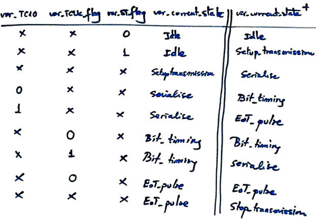 |
Fig. 6. The state logic flowchart is a behavioural interpretation of the truth table CC1 to organise all state transitions and loops. |
Generating the Din odd parity bit will be simply counting the number of ones. And and other statements like composing the frame, shifting and counting bits will be immediate.
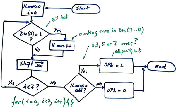 |
Fig. 7. Flowchart to implement a C function for counting ones in var_Din. |
Organise a MPLABX - XC8 IDE project targeting a PIC18F46K22 at location:
C:\CSD\P12\USART\Serial_TX\(files)
| Specifications | Planning | 3. Dev. & 4. test | Prototype | Report |
A) Developing hardware
The application Serial.TX.pdsprj captured in Proteus.
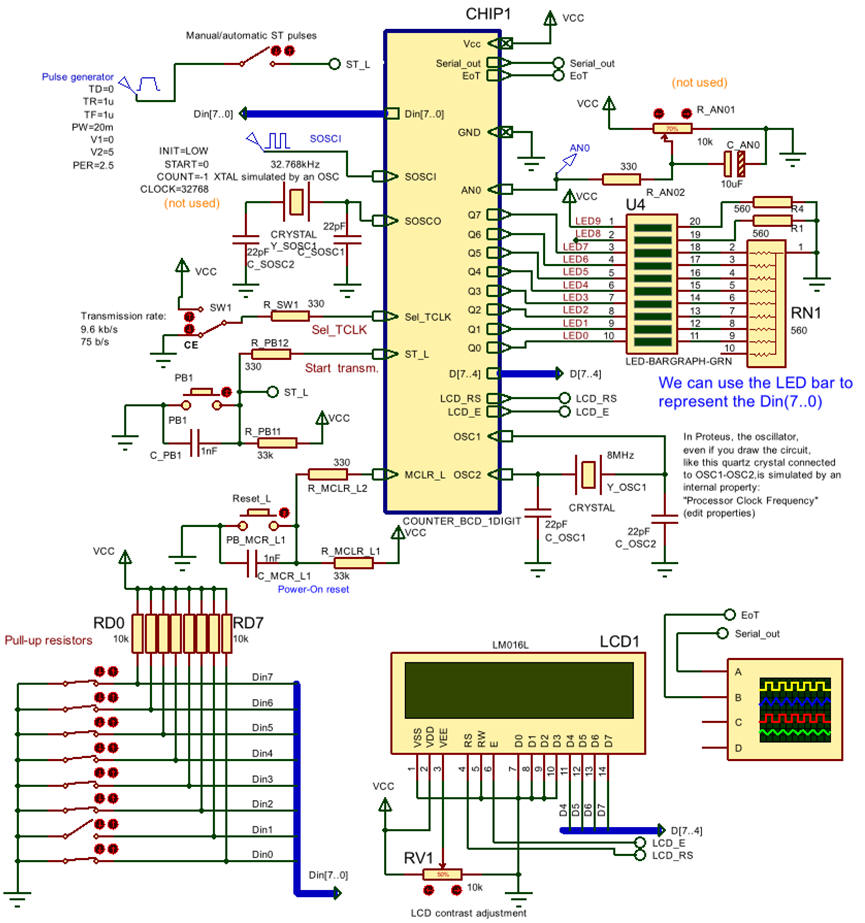 |
Fig. 8. Capturing the circuit in Proteus. |
B) Developing software
The LCD kit software driver, these LCD library files "lcd.c", "lcd.h" from P11, have to be included in the project. The file "config.h" contains all the microcontroller configuration bits. The complete source file for this application Serial.TX.c. Generate the executable (*.hex) and debugging file (*.cof) for Proteus simulations.
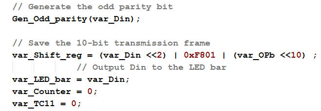 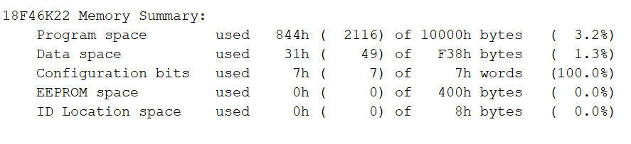 |
Fig. 9. Example of a section of C code in Setup_tranmission state for generating the odd parity bit, composing the frame, visualising Din and initialising the bit counter. Microcontroller resources used in this application: 3.2% of the program memory. |
C) Step-by-step testing
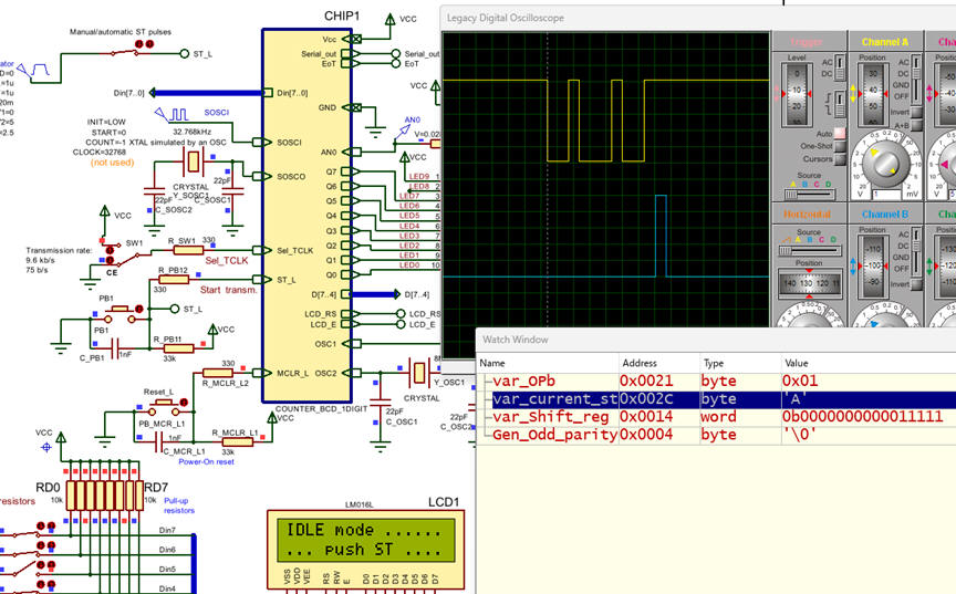 |
Fig. 10. Circuit running on the simulator ready for debugging. |
| Specifications | Planning | Dev. & Test | 5. Prototype | Report |
We can use the VB8012 logic analyser to visualise the transmitted serial frame.
Fig. 11. Picture of the transmitter prototype. |
| Specifications | Planning | Dev. & Test | Prototype | 6. Report |
| Home Term 26/27-Q1 Contact Products Electronic devices and companies Software Books Magazines Instruments DEE Library EETAC DEEL |

|
|
| Web activa des de 09/2001, @ F. J. Robert, Web editat amb Microsoft Expression Web 4. El contingut és un complement als materials d'estudi del curs Circuits i Sistemes Digitals disponibles al campus digital Atenea. Llicència:Reconeixement 4.0 Internacional de Creative Commons |