|
|
Bachelor's Degree in Telecommunications Systems and in Network Engineering |
|
|
|
||
|
|
Advanced project on designing static RAM |
|
|
|
||
Optional supplemental resources Using FPGA synthesisable RAM memory blocks
1. Specifications
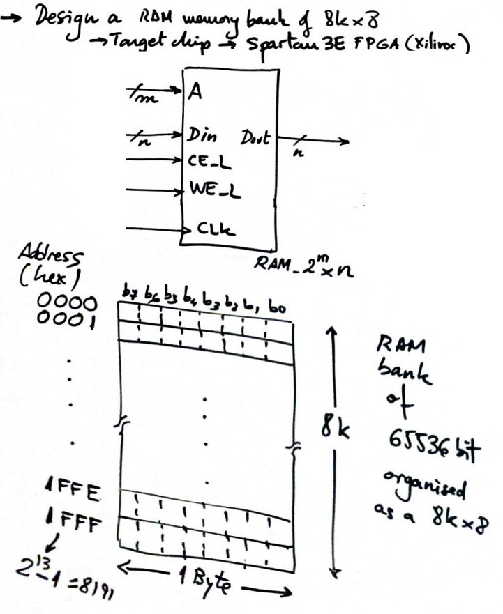
Organise an 8 KB memory bank (28x8 = 65536 bits) using basic RAM block primitives from an specific FPGA family. For instance AMD Spartan 3E.
 |
|
Fig. 1. Symbol of the 8 kB memory bank to be synthesised in an FPGA. |
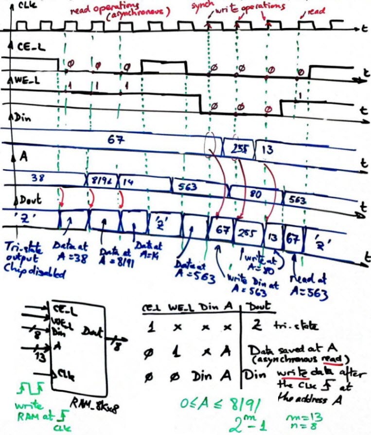
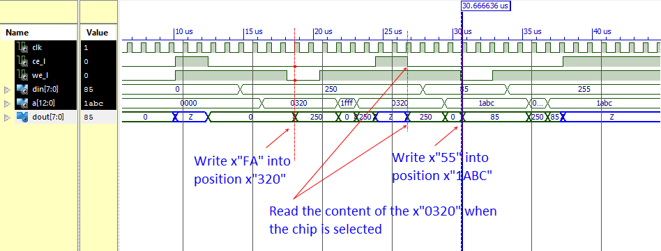
The Fig. 2 represents an example of timing diagram and the way the RAM block is expected to work. Writing operations will be synchronous to the CLK, however, reading will be level sensitive. The output port Dout is available when the chip is enabled (CE_L = '0') presenting the data stored in the memory position A, otherwise it is kept in tri-state.
 |
|
Fig. 2. Example of timing diagram accordingly to the proposed function table. |
- This is the datasheet of the classic RAM chip 6116 to compare features with the RAM blocks available in FPGA.
- The idea of specific and advanced libraries of digital components: IP, intellectual property. These components must be used when optimising chip performance in advanced designs.
- This is how the specific RAM memory in a Xilinx Spartan FPGA works.
- The idea of RAM expansion. How to build larger memory blocks using smaller components of the same kind (plan C2)?
2. Planning
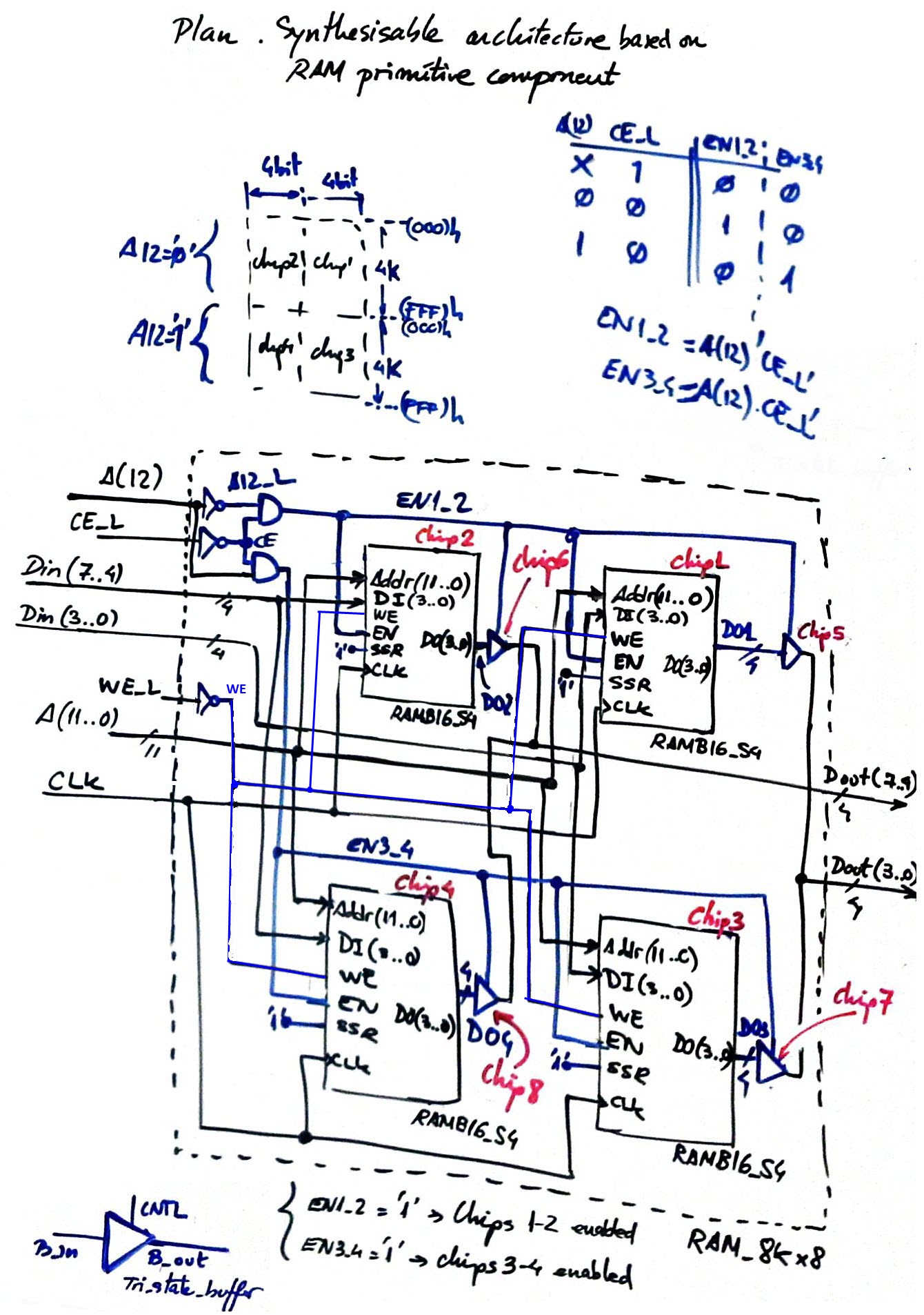
In Fig. 3 there is the basic generic RAM block available in Xilinx Spartan 3 family of FPGA. For instance, when n = 4, m = 12, the block becomes the RAMB16_S4 which is a memory of 16K bits organised as a 4Kx4.
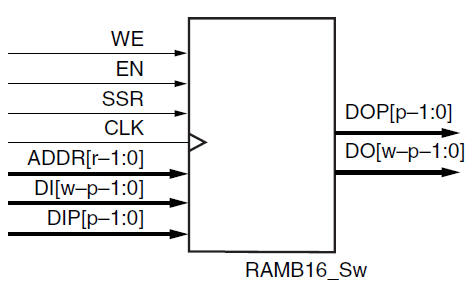 |
Fig. 3. Symbol of the generic 16K bit memory block and the datasheet. |
So, we can organise the expansion of the RAMB16_S4 using 4 of them as in this plan schematic.
Before translating it to VHDL the quadruple tri-state buffer component has to be designed because we want to connect chip outputs together (naturally, not operating at the same time).
3. Development
- Files RAM_8Kx8.vhd, Quad_Tri_state_buffer.vhd.
Run the EDA synthesis project and inspect the RTL schematic. Check the number of RAM blocks used. This is the technology view.
4. Testing
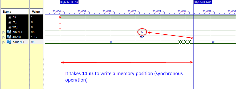
- Example RAM_8Kx8_tb.vhd test bench . Print the timing diagram and interpret the waveforms. Observe how the data is written synchronously, but it can be read immediately after inputting a new memory address.
This a timing diagram showing several write and read operations.
This is the measurement of the writing speed by means of a gate-level simulation.
5. Report
Project report starting with the template sheets of paper, scanned figures, file listings, docx , pptx, or any other resources .
6. Prototyping
Use training boards and perform laboratory measurements to verify how the circuit works.
| Home Term 26/27-Q1 Contact Products Electronic devices and companies Software Books Magazines Instruments DEE Library EETAC DEEL |

|
|
| Web activa des de 09/2001, @ F. J. Robert, Web editat amb Microsoft Expression Web 4. El contingut és un complement als materials d'estudi del curs Circuits i Sistemes Digitals disponibles al campus digital Atenea. Llicència:Reconeixement 4.0 Internacional de Creative Commons |