|
|
Bachelor's Degree in Telecommunications Systems and in Network Engineering |
|
|
|
Analysis of Circuit_W based on logic gates |
| Method I | Method II | Method III | Method IV |
| 1. Specifications | Planning | Developing | Testing | Report |
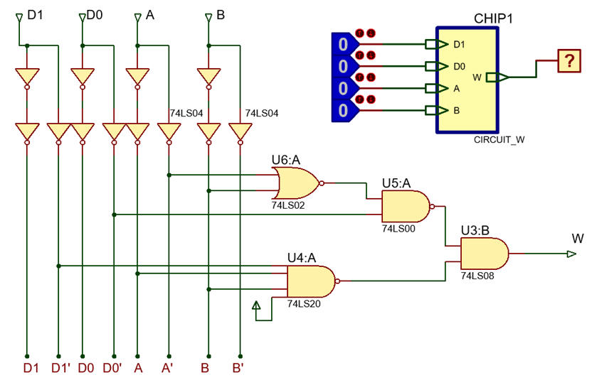
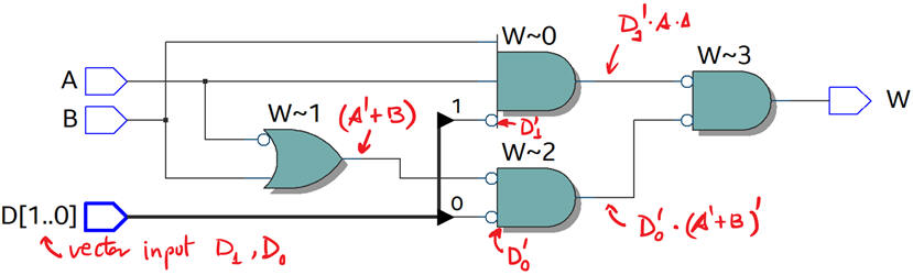
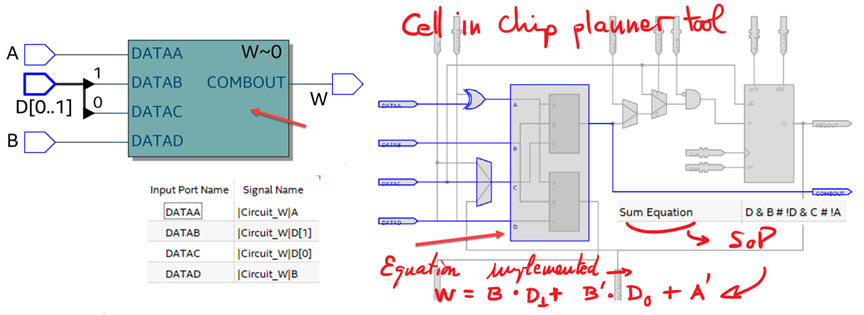
Analyse the section of Circuit_C proposed in P1 naming it as Circuit_W. The symbol and its internal architecture is represented in Fig. 1. Find its truth table using method I. This is a rec. on the idea of circuit analysis.
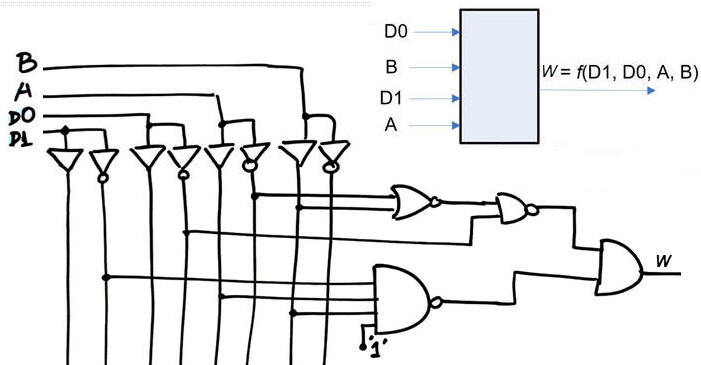 |
| Fig. 1. Circuit_W symbol and internal architecture. |
| Specifications | 2. Planning | Developing | Testing | Report |
Follow our concept map in Fig. 2:
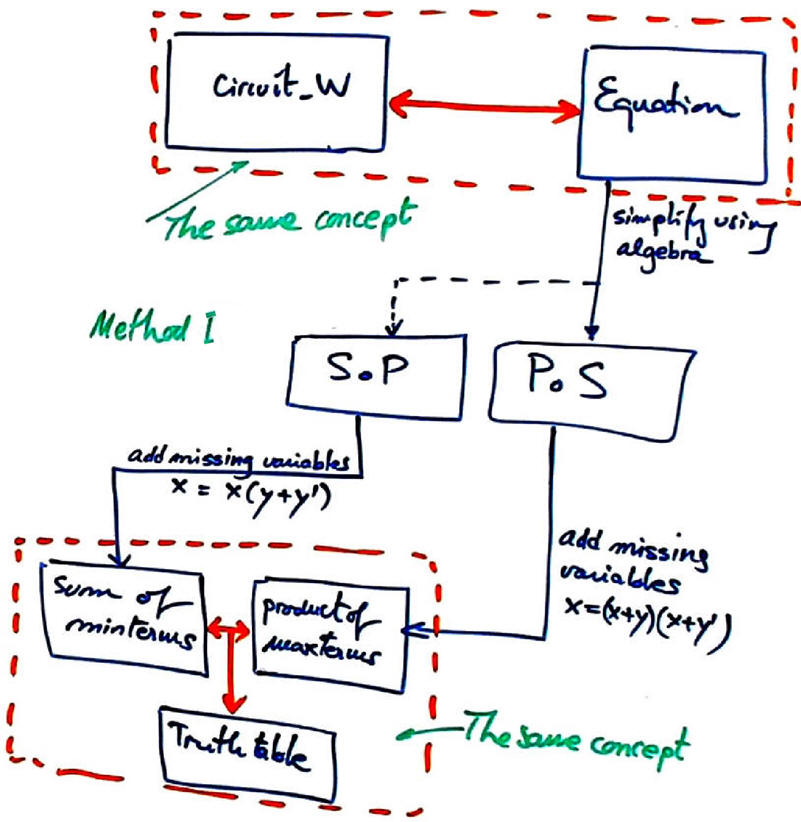 |
| Fig. 2. Plan for the analysis method I. |
-
Firstly, we deduce the circuit's equation: the logic diagram translated to an algebraic equation.
-
Secondly, applying algebra we simplify the circuit equation to obtain PoS (or SoP).
-
Thirdly, we add missing variables to convert sums into maxterms using the identity x = (x+y)·(x+y'), and the final product of maxterms is already the solution.
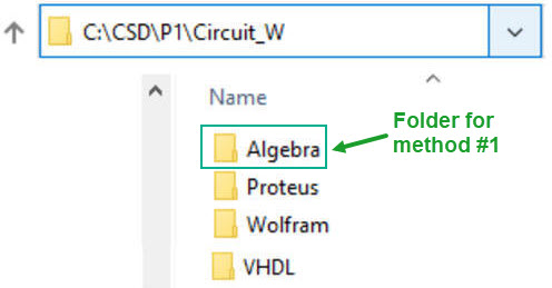
This is the folder where to save your notes, pictures, scanned diagrams and discussion:
C:\CSD\P1\Circuit_W\Algebra\(files)
| Specifications | Planning | 3. Developing | Testing | Report |
This is Circuit_W solution rec. using the proposed analysis method I. The initial concepts of circuit and its translation to an equation:
 |
| Fig. 3. The Circuit_W equivalent equation. |
Now, we can begin the process of simplification using Boole's algebra as follows:
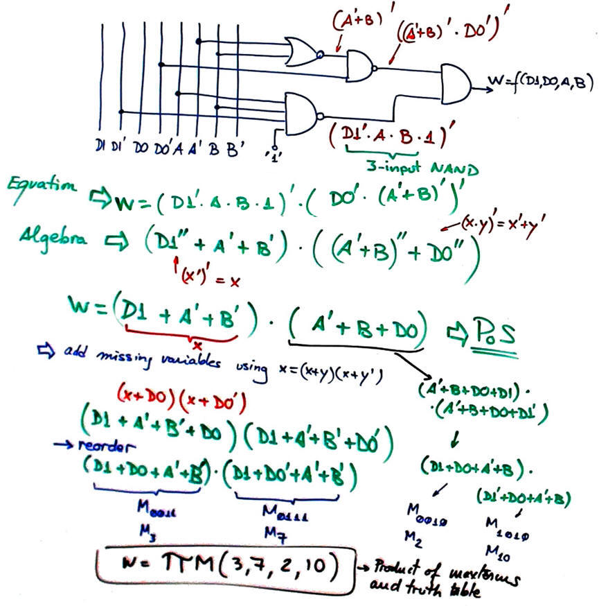 |
| Fig. 4. Simplifying using Boole's algebra to obtain a PoS equation or circuit. |
From the PoS expression in Fig. 4, we can continue converting the sums into maxterms adding in each term the the missing variables and reordering the inputs in the way we like to draw the truth table:
 |
| Fig. 5. The final truth table deduced as a product of maxterms. |
Alternatively, from the circuit equation we obtain a SoP that becomes the sum of minterms adding missing variables in each product using x = x·(y + y') = x·y + x·y'.
| Specifications | Planning | Developing | 4. Testing | Report |
This time, testing the validity of the truth table will be simply comparing solutions from other methods.
| Specifications | Planning | Developing | Testing | 5. Report |
| Method I | Circuit_W method II | Method III | Method IV |
| 1. Specifications | Planning | Developing | Testing | Report |
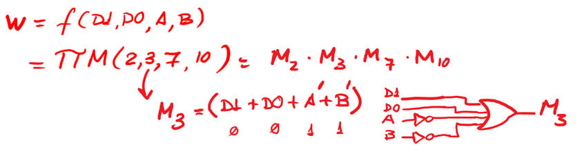
Our goal is to deduce Circuit_W truth table W = f (D1, D0, A, B) by means of running Proteus simulations (method II). This is a tutorial and a video rec. on how to proceed with Proteus to deduce a circuit truth table. Component models can be from these two options but do not mix components from different libraries in the same schematic:
Option #1: Classic LS-TTL
Option #2: Classic CMOS
|
|
|
Fig. 1. Symbol and internal architecture of Circuit_W. |

| Specifications | 2. Planning | Developing | Testing | Report |
Draw a plan for this analysis method II. It is possible to model logic gates using CMOS or TTL-LS libraries. Draw all gates using the same library.
|
|
|
Fig. 2. This sketch explains the plan to follow to deduce the Circuit_W truth table. You must add/modify/delete the circuit step by step (one gate at a time) and run to check that it works correctly. |

This is the project location:
C:\CSD\P1\Circuit_W\Proteus\(Circuit_W.pdsprj and other files)
| Specifications | Planning | 3. Developing | Testing | Report |
Use a mouse with your portable computer to make it easier to draw the circuit and navigating through the many tabs.
Find a similar circuit to copy and adapt from this DIGSYS web. Change its name and save it in the given directory.
In this tutorial we will use either TTL-LS (74LS) or CMOS series 4000B libraries of classic components. For instance: a 3-input NOR gate in classic CMOS 4000 technology is the 4025B; the same 3-input NOR in TTL-LS technology is 74LS27. Do not mix gates from different logic families, they may not be electrically compatible.
This is an example "Circuit_W.pdsprj" capture using LS-TTL (VCC = 5 V, VGND = 0 V). Print the captured circuit to demonstrate that you are able to draw circuits as shown in Fig. 3. This is the same "Circuit_W.pdsprj" capture using CMOS (VDD = 15 V, VSS = 0 V).
|
|
|
Fig. 3. Example of picture showing how the Circuit_W is captured in Proteus tool. |
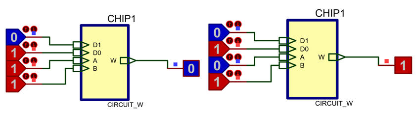
Run simulations applying all the binary combinations in order to complete your truth table.
|
|
|
Fig. 4. Simulation results when applying input binary combinations "0111" and "0101". We can observe that "0111" generates the maxterm M7 and "0101" generates the minterm m5. |
Write down your solution as a truth table or its equivalent canonical equations sum of minterms or product of maxterms.
|
|
|
Fig. 5. Problem solution using the canonical form of product of maxterms. |
| Specifications | Planning | Developing | 4. Testing | Report |
In CSD verifying your solutions means self-assessing your results. This is why comparing results from other methods is the best idea. For instance method I or method IV.
In this way, this verification section (a sheet of paper) has to say something as simple as:
"My Circuit_W analysed using method II (Proteus) generates the same truth table that was obtained using method I".
| Specifications | Planning | Developing | Testing | 5. Report |
Follow this rubric for writing reports. This is an example that shows how to write a report of a circuit analysis using the method II based on Proteus simulations.
| Method I | Method II | Circuit_W Method III | Method IV |
| 1. Specifications | Planning | Developing | Testing | Report | Prototype |
Find the truth table of Circuit_W represented in Fig. 1 using VHDL synthesis and simulation tools.
|
|
| Fig. 1. Symbol and internal architecture of Circuit_W to be analysed. |
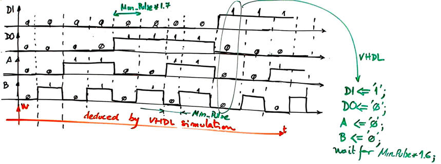
Draw an example of timing diagram showing how to drive inputs, so that the truth table (circuit output) can be deduced using a VHDL testbench in ModelSim tool.
|
|
| Fig. 2. Example timing diagram showing some input combinations and how they can be translated into a VHDL file. In this project we must run the simulation for all the input combinations to be able to deduce the circuit's truth table. |
| Specifications | 2. Planning | Developing | Testing | Report | Prototype |
The plan requires, as in method IV (WolframAlpha) or method I (algebra), obtaining the circuit's equation that this time will be translated literally to VHDL.
Part I: circuit synthesis
- Find a similar file to copy and adapt. For example from this EDA tutorial on Quartus Prime installation. Rename and save it as "Circuit_W.vhd" at this project location:
C:\CSD\P1\Circuit_W\VHDL\(files)
- Translate your circuit equation into VHDL using the Notepad++ enriched editor.
- The tool for synthesising the equation will be Intel Quartus Prime. The tool for simulating the circuit will be ModelSim Intel Starter Edition. Select an Intel target chip, for example, the CPLD MAX II EPM2210F324C3 chip.
|
|
| Fig. 3. Initial ideas on planning the solution. Add many more details on the sequence of steps required to obtain the final truth table. Explain also the concepts involved in this flow. |
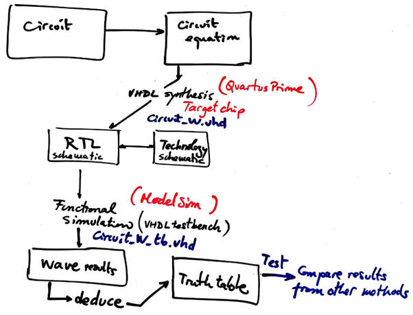
- Start a Quartus Prime project and synthesise the circuit.
- Examine, print and discuss the RTL schematic.
- Examine and discuss the technology schematic. How many resources from the FPGA are used in this circuit?
Part 2: circuit simulation to be developed in the second part of this laboratory session below:
- Draw a VHDL testbench fixture for the chip under test. In two steps:
-
Generate an skeleton testbench in Quartus Prime. Move it to the project folder and rename it as "Circuit_W_tb.vhd".
-
Complete the stimulus process with some input activity, for example with some signals from Fig. 2.
- Run the simulation and examine the wave analyser results.
- Complete all the combinations and write down the circuits truth table.
- Check the truth table comparing results from other methods.
| Specifications | Planning | 3. Developing | Testing | Report | Prototype |
Part 1: Circuit synthesis
Start obtaining the equivalent circuit equation using paper, as in Fig. 4.
|
|
|
Fig. 4. Analysis gate by gate in order to find the equivalent algebraic equation. |

NOTE: In CSD use the Notepath++ enriched text editor, a very convenient free tool for writing VHDL and C files. Another free enriched editor is Scriptum from the company HDL Works.
Find a similar file to copy and adapt. Rename and save it as "Circuit_W.vhd" at this project location: Translate your circuit equation into VHDL using the Notepad++ enriched editor.
|
|
| Fig. 5. Project location and file name. |

This is a VHDL source file example "Circuit_W.vhd".
|
|
| Fig. 6. Example of circuit description printing and indications. |

Start a new synthesis project targeting a commercial programmable logic device (PLD) or field programmable gate array (FPGA) chip. Here you have several devices available in our labs for experimentation. For instance, let us select an Intel CPLD MAX II EPM2210F324C3 chip.
-
Project name: Circuit_W_prj
-
Top entity: Circuit_W
|
|
| Fig. 7. Quartus Prime new project wizard. Pick up for instance a MAXII, MAX10 or Cyclone target chip. |


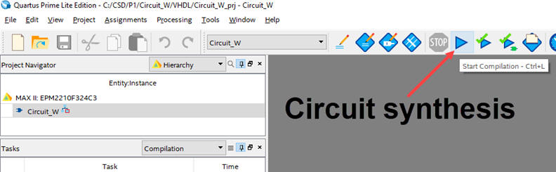
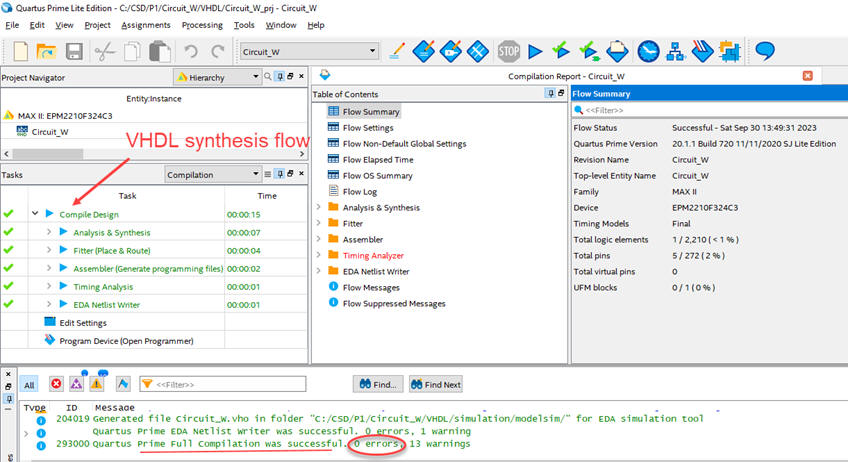
Run the circuit synthesis flow to obtain the circuit.
|
|
| Fig. 8. Synthesis, start compilation top icon and final summary indicating zero errors. |
Represent your circuit visualising the RTL schematic (ideal) and also the technology view (real).
|
|
| Fig. 9. Tools for visualising the circuit synthesised. |
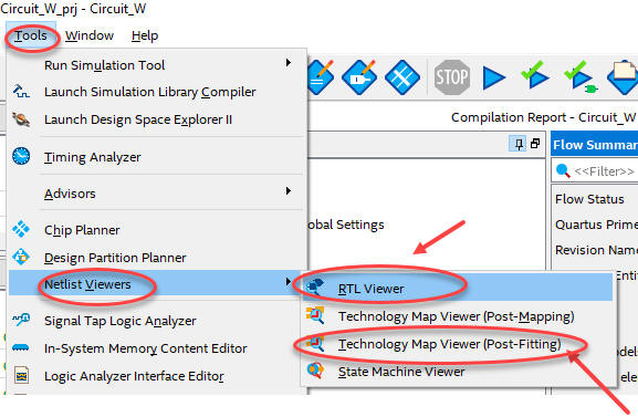
Print the circuits using snipping tool (or any other similar tool like Snagit from TechSmith). Discuss differences between the two schematics. How many resources are used (logic cells or macrocells)?
|
|
| Fig. 10. RTL example picture. |
Finally, as shown in Fig. 11, the real circuit is synthesised in a single LUT cell using SoP equation minimised by Quartus Prime.
|
|
| Fig. 11. Technology view when targeting a MAX II chip. |
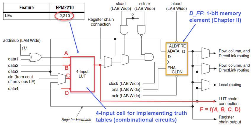
It is a good time to browse the MAXII datasheet and figure out some target chip details. How many resourses are used in this synthesis? What is a logic element? What is a look-up table (LUT)?
|
|
| Fig. 12. Example of logic cell to implement functions. MAX II EPM2210F324C3 contains 2210 logic elements. |
Part 2: Simulation using a VHDL testbench
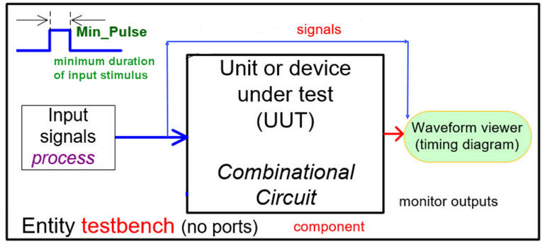
Now that we have the circuit synthesised by Quartus Prime in a MAX II device, it must be simulated to obtain its truth table. Generate a testbench template in Quartus Prime. Fig. 13 represents the idea behind a VHDL testbench.
|
|
| Fig. 13. The VHDL testbench concept. |
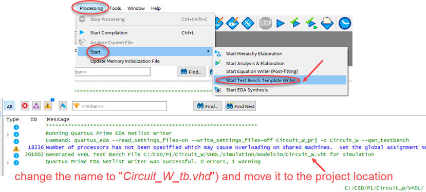
In a first step, obtain the testbench template. Rename the file from "Circuit_W.vht" to "Circuit_W_tb.vhd" and move it to the project location folder.
|
|
| Fig. 14. Obtaining the testbench template. |
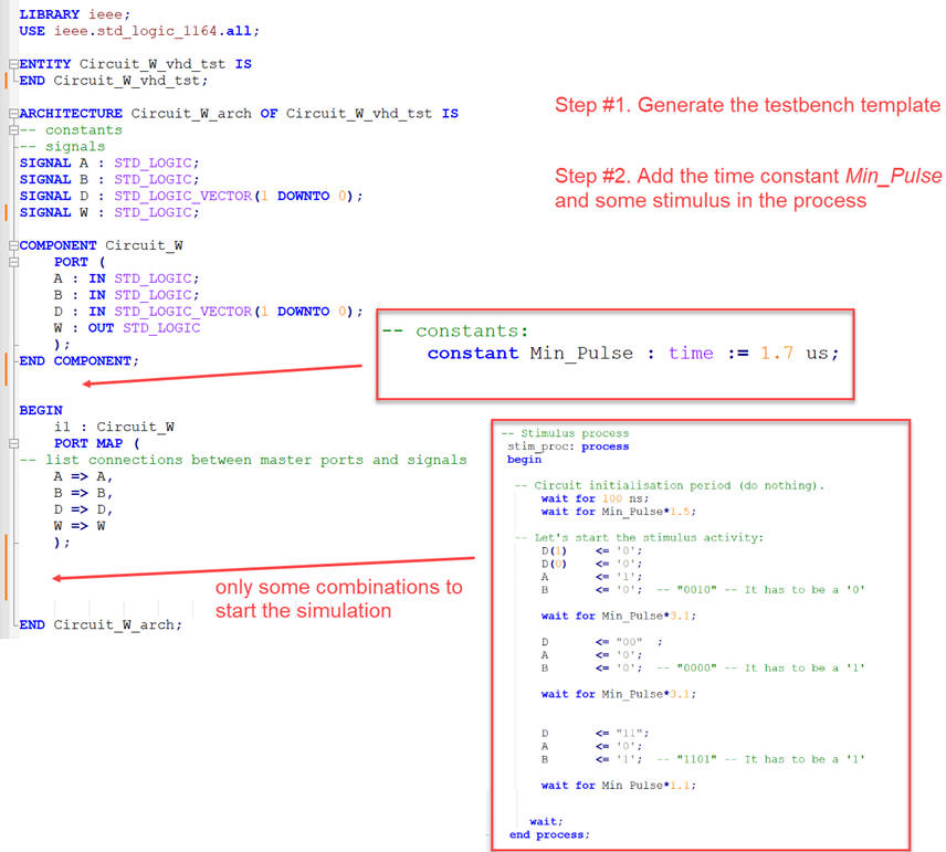
In a second step, using the example timing diagram in Fig. 2, translate into VHDL the stimulus signals into a process and set the constant Min_Pulse. This is a VHDL testbench example "Circuit_W_tb.vhd" from which you can copy only the stimulus process and Min_Pulse constant.
|
|
| Fig. 15. You can edit the testbench schematic in VHDL in two steps. |
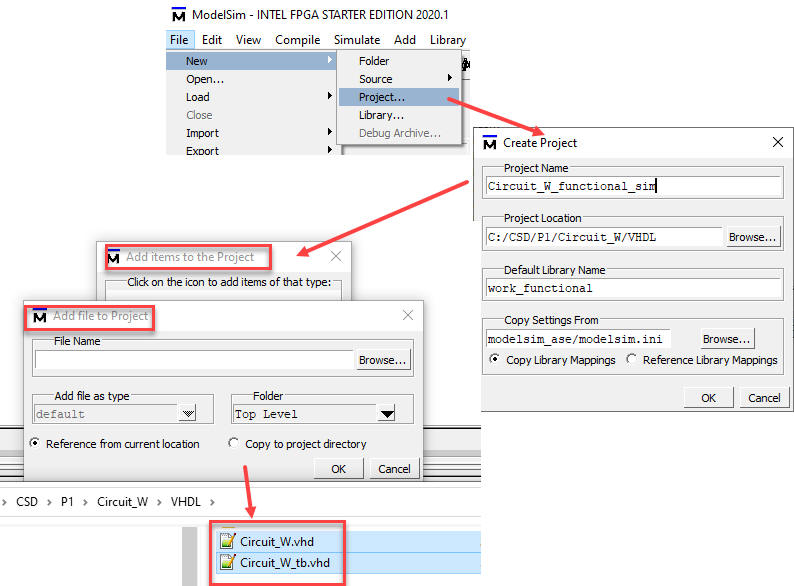
Start a project in ModelSim Intel Starter Edition (or in Xilinx ISim or in Active-HDL).
|
Note: remember to change preferred colours in ModelSim when using it for the first time. White background must be used to write clear annotations on the pictures and save ink when printing. |
Project location: C:\CSD\P1\Circuit_W\VHDL\(the same location as above for synthesis)
Project name: Circuit_W_functional_sim
Project library: work_functional
|
|
| Fig. 16. Start a new project for functional (ideal) simulations. Be aware to add the two VHDL files composing the testbench in Fig 13. |
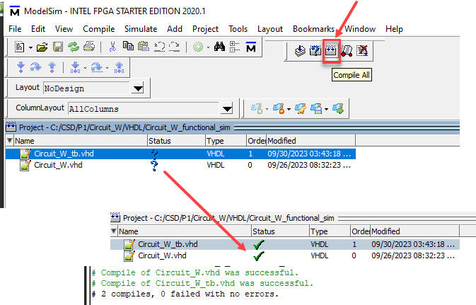
It is time to compile all the project, the two VHDL files: the testbench and the unit under test. You must get green ticks in the status column when zero errors.
|
|
| Fig. 17. Compile all and get ready for starting the simulations. |
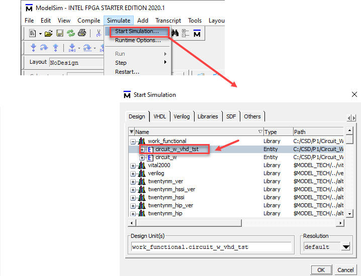
Everything is ready now to start running a simulation considering the top entity where the stimulus process for the UUT is written.
|
|
| Fig. 18. Start simulations selecting the testbench top entity in the hierarchy. |
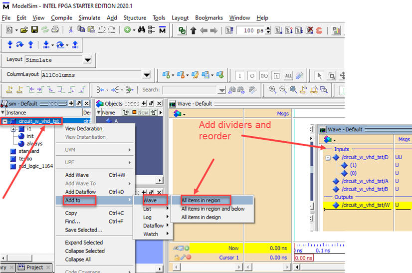
Add signals of interest to the wave diagram using the right mouse button. This operation is like preparing an initial setting of a logic analyser instrument.
|
|
| Fig. 19. Add the signals of interest to the timing diagram. |
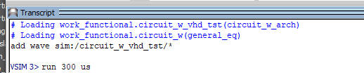
Run the simulator for a convenient time (longer than the stimulus duration) and adjust the grid and the time units. Configure your wave diagram so that you do not see the vertical grid lines, as shown in Fig. 20 and get a clearer picture.
|
|
| Fig. 20. Add run command in the console window and adjust the grid and time units. |

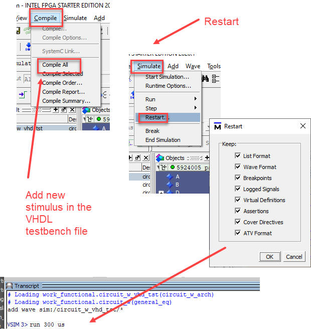
Step by step: once you get results correctly, add new stimulus and complete all combinations recompiling the project and restarting the simulations.
|
|
| Fig. 21. Restarting the simulations. |
Run the full simulation process and extract the truth table from the inspection of the logic analyser display (wave window) using time cursors and adding handwritten comments over the pictures after printing, as represented in Fig. 22.
|
|
| Fig. 22. Example of commented waveforms from ModelSim. |
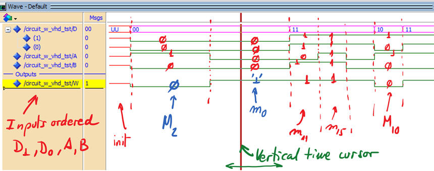
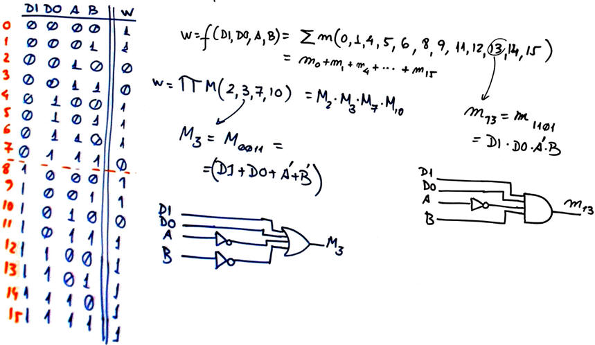
Fig. 23 shows the final truth table result.
|
|
| Fig. 23. Circuit_W truth table and its canonical equations. |
| Specifications | Planning | Developing | 4. Testing | Report | Prototype |
Verification of the truth table. Compare your truth table with results from other methods. For instance, from method II or method IV in Lab1_1 or method III in L1_3. In this way, this section has to say something as simple as
"My Circuit_W generates the same truth table using method III and method II".
| Specifications | Planning | Developing | Testing | 5. Report | Prototype |
Follow this rubric for writing reports.
| Specifications | Planning | Developing | Testing | Report | 6. Prototype |
These are basic ideas consisting of drawing a top schematic to adapt the project to the specific board hardware. Because it is a hierarchical multiple-file design, any circuit based on our design plan C2 can be copied and adapted to be the top entity. We recommend to build this prototype after having completed P3 projects.
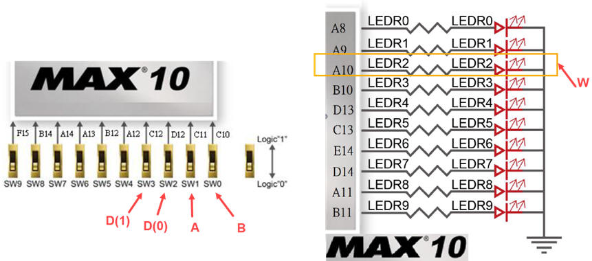
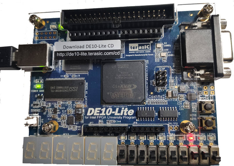
DE10-Lite board. This page MAX10 DE10 Lite contains information and the used manual. This is another complete tutorial example introducing and prototyping on the DE10-Lite.
Fig. 24 shows the schematic to adapt the Circuit_W to the FPGA MAX10 populating the DE10-Lite board. All our prototype adaptations will be named in the same way: we will identify the component under design "Circuit_W" and add "_top" suffix.
Prototype location:
C:\CSD\P1\Circuit_W\DE10_Lite\(files)
 |
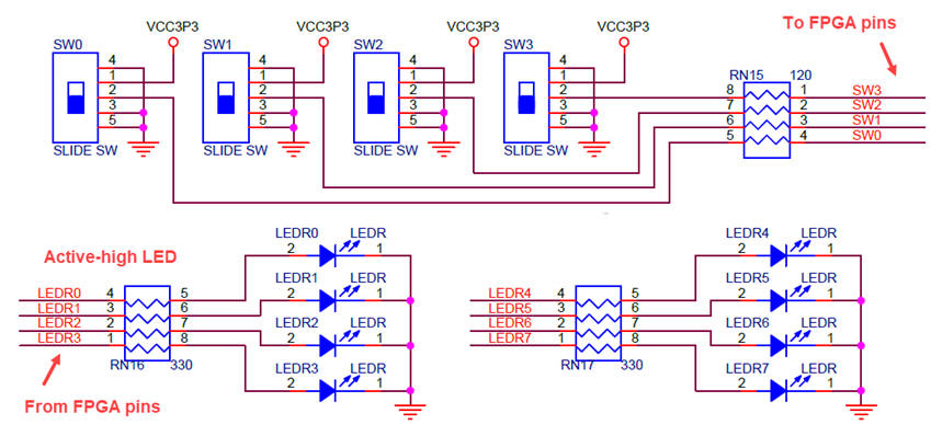
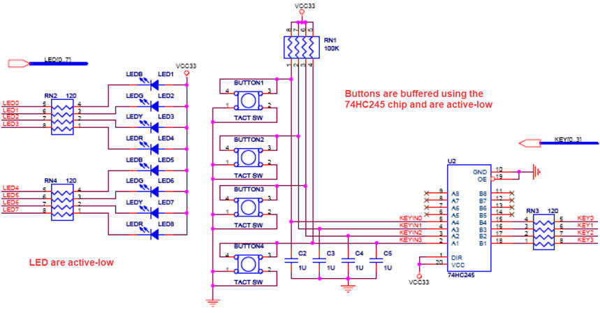
Fig. 24. Schematic consisting of a top entity with the component and the glue logic to adapt inputs and outputs to the board's hardware. Studying the schematics we see that the switches are connected through a series 120 W resistor to the FPGA pins for protection purposes (pins are also available at expansion connectors).
The two keys, KEY0 and KEY1, are buffered using a SN74LVC2G17 chip and they are active-low including as well an RC debouncing filter. |
  |
|
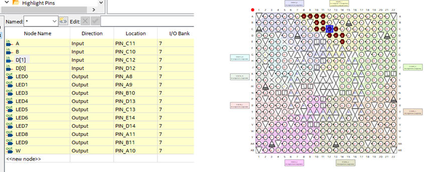
Using pin planner tool at Quartus Prime navigator we connect signals to FPGA pins. We can export the asignment to a file to keep it save.
|
|
| Fig. 25. Pin planner tool allows assigning circuit signals to FPGA pins. |

This zipped file Circuit_W contains all the required files for implementing project. As shown in Fig. 26 the programmer tool is used to download the configuration file to the FPGA target chip.
|
| Fig. 26. Programmer and circuit running for final checking and verification. |

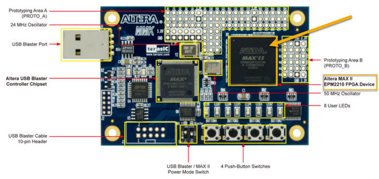
MAXII Micro kit. This is the board MAXII Micro kit board. Rec.
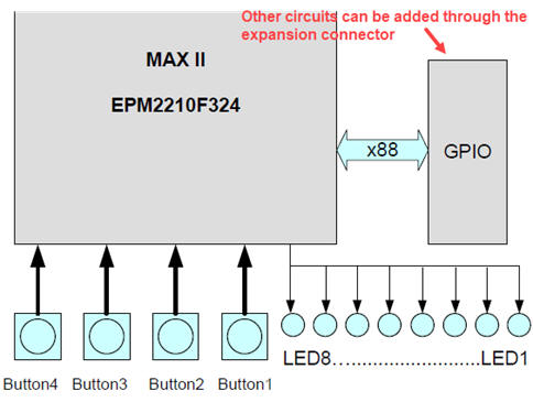
Fig 27 shows the training board populated with a MAX II chip. Expansion connectors in areas A and B can be soldered so that many more FPGA I/O pins are available for prototyping designs.
Prototype location:
C:\CSD\P1\Circuit_W\MAXII_Micro_kit\(files)
|
|
| Fig. 27. Lab training board populated with MAX II EPM2210F324C3 for experimentation. |
As shown in the top schematic in Fig. 28, for this simple project only the buttons and a single LED will be used.
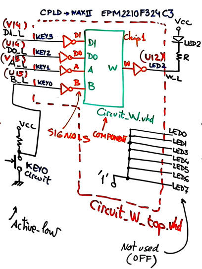 |
Fig. 28. Schematic consisting of a top entity with the component and the glue logic to adapt inputs and outputs to the board's hardware.
|
 |
|
This is the zipped project Circuit_W containing all the required files to complete this experiment.
| Method I | Method II | Method III | Circuit_W method IV |
| 1. Specifications | Planning | Developing | Testing | Report |
Our goal is to deduce Circuit_W truth table W = f (D1, D0, A, B) using WolframAlpha numerical engine (method IV). Video rec. on how to proceed with WolframAlpha.
|
|
|
Fig. 1. Symbol and internal architecture of Circuit_W. |
| Specifications | 2. Planning | Developing | Testing | Report |
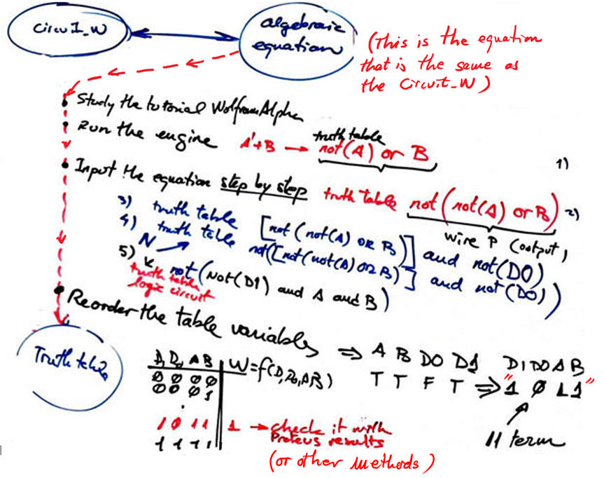
Draw a plan, a flowchart, a bullet list, for obtaining and checking your solution. For this method, the key point is to input the circuit equation step by step , one logic gate at a time, while running the engine to check that there are no errors when interpreting the equation.
|
|
|
Fig. 2. Proposed method IV detailed flowchart to carry out this analysis project. |
This is a convenient location for this project:
C:\CSD\P1\Circuit_W\Wolfram\(files)
Files may include your written equations "Circuit_W_equ.txt" and other files like printed result images.
| Specifications | Planning | 3. Developing | Testing | Report |
Analyse the circuit and obtain its logic equation, as shown in Fig. 3. It is the same analysis and the same initial equation shared for all three method I, method III and method IV.
|
|
|
Fig. 3. Analysis gate by gate in order to find the equivalent algebraic equation corresponding to Circuit_W. |

Start writing simpler equations in a text file and try them in WolframAlpha. This file "Circuit_W_equ.txt" contains some equations to copy and paste into WolframAlpha. We use Notepad++ as enriched text editor for writing text equations.
Run WolframAlpha engine to get results: "truth table", "logic circuit".
Print WolframAlpha truth table and logic circuit in a sheet of paper.
|
|
|
Fig. 4. Example of printed and interpreted results from WolframAlpha. |

Reorder columns W = f (D1, D0, A, B) and complete the circuit's truth table identifying all minterms and maxterms.
|
|
|
Fig. 5. Problem solution, the Circuit_W truth table, presented using the canonical form sum of minterms. |

| Specifications | Planning | Developing | 4. Testing | Report |
Compare results with other methods. For instance method I or method II solved above.
In this way this section has to say something as simple as:
"My Circuit_W generates the same truth table when solved using method IV and method II".
| Specifications | Planning | Developing | Testing | 5. Report |
Follow this rubric for writing reports.
| Home Term 26/27-Q1 Contact Products Electronic devices and companies Software Books Magazines Instruments DEE Library EETAC DEEL |

|
|
| Web activa des de 09/2001, @ F. J. Robert, Web editat amb Microsoft Expression Web 4. El contingut és un complement als materials d'estudi del curs Circuits i Sistemes Digitals disponibles al campus digital Atenea. Llicència:Reconeixement 4.0 Internacional de Creative Commons |