|
|
Bachelor's Degree in Telecommunications Systems and in Network Engineering |
|
Chapter 3 problems |
- D3.4 - |
Pattern detector (µC - C) |
V1 |
1. Specifications
Our aim is to implement a circuit to detect the binary pattern "0110" received from a transmitter bit stream at input T using a µC PIC18F46K22, C language and our programming style. Fig. 1 shows the symbol of this pattern_detector circuit.
 |
|
Fig. 1. Symbol (adapt it from D2.4). |
The same project designed using hardware is stated in D2.4.
The detected pattern is an option, for instance:
-Option #1: "0110"
-Option #2: "11010"
Use the option given by your instructor. The remaining indications in this page are adapted to the pattern in option #1.
When the sequence "0110" is detected, output Z goes high for one CLK period. Two or more adjacent patterns can also be detected as in this bit stream sequence: "01101101101..."
To make the design simpler, we will assume:
- Both, the T bitstream and the CLK are of the same frequency fCLK.
- The T bitstream signal is delayed half period (180°) with respect the CLK, to be able to sample stable data on the CLK's rising edges.
- The detector is working continuously once the power supply is turned on.
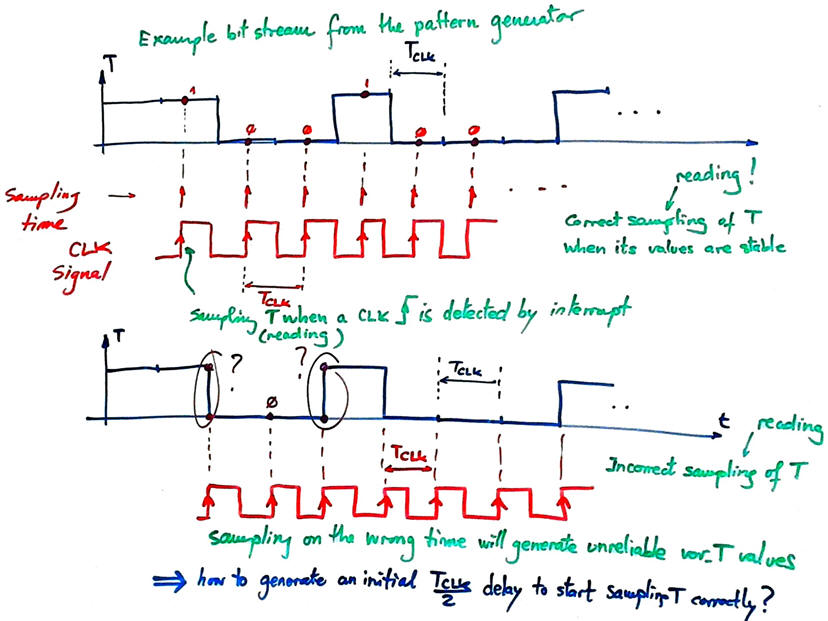
The best way to start, is to try imagining how the output will be for a given bitstream, as represented in Fig. 2.
 |
| Fig. 2. Example of timing diagram. |
2. Planning
Let us build the product organising several design phases, and several steps within each phase if necessary.
Design phase #1: basic features
Some ideas to kick off the project and organise it. Apply the FSM architecture adaptation L10.1 to this problem.
Project location:
C:/CSD/P10/pattern_detector/files)
NOTE: It is clear that your preliminary step in this project is to learn how to use a pattern generator in Proteus. You have at least three options: the instrument pattern generator itself; the Easy HDL scripting language; and the generic function generator working as an arbitrary digital waveform generator. They are described in the unit Proteus. Try to learn how to configure bit stream and capture them in the oscilloscope or logic analyser instruments. This instrument will be used to stimulate your Pattern_detector circuit (you already had to do it as a PROCESS in your VHDL testbench in D2.4).
Another important issue for starting the design and the adaptation of the state diagram to this project is the initial delay of half bit time ( TCLK/2) before starting sampling/reading the serial input T. You have to be sure that you are capturing T logic values at fCLK when they are stable, never near a signal transition.
A) Planning hardware
Copy and adapt a circuit from a convenient tutorial project and name it "pattern_detector.pdsprj". Assign pins to inputs and outputs accordingly to one of the following options (your instructor will tell you which):
Pin assignment option #1:
CLK --> RB1
T --> RB6
Z --> RC7
Pin assignment option #2:
CLK --> RB2
T --> RA2
Z --> RD7
Pin assignment option #3:
CLK --> RB0
T --> RB7
Z --> RC4
Draw the hardware schematic. Buttons and switches, resistors, inputs, outputs, reset circuit MCLR_L and quartz crystal oscillator of 8 MHz. Explain how to configure inputs and outputs in init_system().
How to generate example bit streams in Proteus?
B) Planning software
Draw the flowchart of the general program organisation.
Draw the hardware/software diagram indicating the required RAM variables and how the FSM is solved in software.
Infer the state diagram governing the machine.
Explain how to poll (read) input T in read_inputs() using bitwise operations. Explain how to measure how many times per second this input is read.
Explain how to drive output pins in write_outputs().
Draw the truth tables and their equivalent flowcharts for state_logic() and output_logic() functions.
How the interrupt service routine ISR() is used in this application? Draw its flowchart.
Developing & testing (debugging)
Develop and test (debugging) the project capturing the hardware circuit in Proteus and writing the C source code.
| Note: Step-by-step tactical approach for developing and testing the project: Read one input at a time and run to check that the voltage value is correctly captured as a valid digital value in RAM memory. Write one output at a time and run to check that your code is correct to light the LED connected at the output pin. |
Design phase #2: LCD display
Add an LCD to show messages, such text, for example: "no input data", "pattern detected", etc. A number will indicate the number of times the pattern is detected in the incoming bit stream.
Project location:
C:/CSD/P11/pattern_detector_LCD/files)
Design phase #3: Using TMR2 peripheral subsystem
Use the TMR2 to replace external CLK interrupts.
Project location:
C:/CSD/P12/pattern_detector_LCD_TMR2/files)
Chapter 3 problems |
- D3.4 - |
Pattern detector (µC - C) |
V2 |
1. Specifications (Version #2)
Design phase #1: pattern detector, synchronisation and noise filtering
Our aim is to implement a circuit to detect the binary pattern "0110" received from a transmitter bitstream at input T using a µC PIC18F46K22, C language and our programming style. The experiment is sketched in Fig. 1.
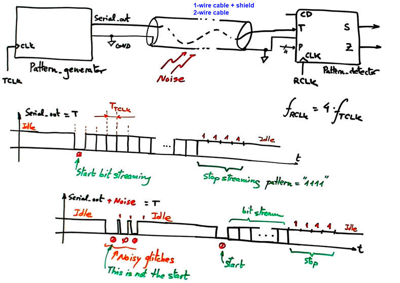 |
Fig. 1. Serial pattern generator and detector experiment. |
The same project designed using hardware is stated in D2.4.
We can use a simple 1-wire shielded cable or a twisted-pair cable to connect the transmitter and receiver units. The pattern generator block may be like presented in D3.22. In this experiment the transmitter TCLK signal is not used, therefore we have to imagine some kind of synchronisation mechanism to allow sampling T when it is stable away from transitions. In order to adjust sampling time in the middle of each transmitted bit, the receiver RCLK frequency is four times the transmitter frequency.
NOTE: It is clear that your preliminary step in this project is to learn how to use a pattern generator in Proteus. You have at least two options: the instrument pattern generator itself or the Easy HDL scripting language, both described in the unit Proteus. Try to learn how to configure bit stream and capture them in the oscilloscope or logic analyser instruments. This instrument will be used to stimulate your Pattern_detector circuit (you already had to do it as a PROCESS in your VHDL testbench in D2.4).
When there is no transmission, the receiver is sampling '1' and is kept idle as it is the transmitter.
The noise filter mechanism may be conceived as shown in Fig. 2: when the first '0' is detected, the receiver will wait for two RCLK to sample another value. If this new sample is '0' it is effectively the start bit of a serial transmission by the pattern generator. If this sample is '1', it means that the first '0' detected was a glitch and thus there is no transmission.
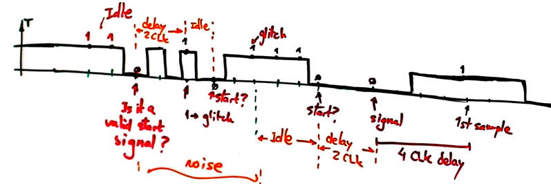 |
| Fig. 2. Receiver signals and the idea of filtering noise. |
And the acquisition of the bit stream will consist of sampling T every four RCLK periods, as shown in Fig. 3.
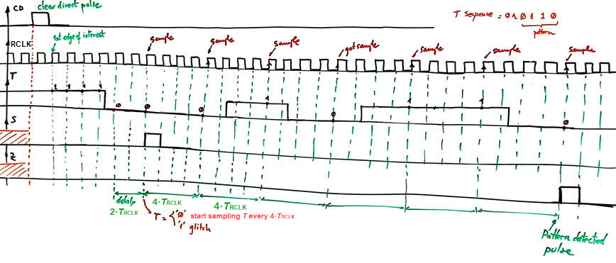 |
| Fig. 3. Receiver signals and pattern identification. |
Output S goes high for one RCLK period as a flag to indicate that bit streaming is starting.
When the pattern "0110" is detected output Z goes high for one RCLK period. Two or more adjacent patterns can also be detected as in this bit stream sequence: "01101101101...". We may also consider detecting anyone of the 16 different patterns, thus P indicating the code to detect is another input to the circuit.
When four '1' are detected consecutively (pattern "1111"), it means that the transmitter has stopped emitting or something went wrong with the bits stream and thus, the receiver must go back to idle.
2. Planning
Let us build the product organising several design phases, and several steps within each phase if necessary.
Design phase #1: basic features
Some ideas to kick off the project and organise it. Apply the FSM architecture adaptation L10.1 to this problem.
Project location:
C:/CSD/P10/pattern_detector/files)
A) Planning hardware
Copy and adapt a circuit from a convenient tutorial project and name it "pattern_detector.pdsprj". Assign pins to inputs and outputs accordingly to one of the following options (your instructor will tell you which):
Pin assignment option #1:
CLK --> RB1
T --> RB6
Z --> RC7
S --> RA3
P --> RC(3..0)
Pin assignment option #2:
CLK --> RB2
T --> RA2
Z --> RD7
S --> RC5
P --> RD(3..0)
Pin assignment option #3:
CLK --> RB0
T --> RA3
Z --> RC4
S --> RD2
P --> RB(7..4)
Draw the hardware schematic. Buttons and switches, resistors, inputs, outputs, reset circuit MCLR_L and quartz crystal oscillator of 8 MHz. Explain how to configure inputs and outputs in init_system().
How to generate example bit streams in Proteus?
B) Planning software
Draw the flowchart of the general program organisation.
Draw the hardware/software diagram indicating the required RAM variables and how the FSM is solved in software.
Infer the state diagram governing the machine.
Explain how to poll (read) input T in read_inputs() using bitwise operations. Explain how to measure how many times per second this input is read.
Explain how to drive output pins in write_outputs().
Draw the truth tables and their equivalent flowcharts for state_logic() and output_logic() functions.
How the interrupt service routine ISR() is used in this application? Draw its flowchart.
Developing & testing (debugging)
Develop and test (debugging) the project capturing the hardware circuit in Proteus and writing the C source code.
| Note: Step-by-step tactical approach for developing and testing the project: Read one input at a time and run to check that the voltage value is correctly captured as a valid digital value in RAM memory. Write one output at a time and run to check that your code is correct to light the LED connected at the output pin. |
Design phase #2: LCD display
Add an LCD to show messages, such text, for example: "no input data", "pattern detected", etc. A number will indicate the number of times the pattern is detected in the incoming bit stream.
Project location:
C:/CSD/P11/pattern_detector_LCD/files)
Design phase #3: Using TMR2 peripheral subsystem
Use the TMR2 to replace external CLK interrupts.
Project location:
C:/CSD/P12/pattern_detector_LCD_TMR2/files)
| Home Term 26/27-Q1 Contact Products Electronic devices and companies Software Books Magazines Instruments DEE Library EETAC DEEL |

|
|
| Web activa des de 09/2001, @ F. J. Robert, Web editat amb Microsoft Expression Web 4. El contingut és un complement als materials d'estudi del curs Circuits i Sistemes Digitals disponibles al campus digital Atenea. Llicència:Reconeixement 4.0 Internacional de Creative Commons |