Chapter 3 problems |
- D3.2 - |
Stepper motor controller (µC - C) |
1. Specifications
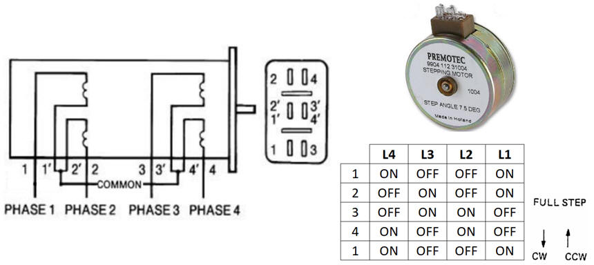
Our aim is to design the digital control unit (Stepper_cntl) for the "9904 112 31004" stepping motor from Premotec shown in Fig. 1 as an application of FSM adaptation to µC. Our target microcontroller is the PIC18F4520.
Another typical stepper motor is the NEMA 17. Nowadays stepper motors can be found in computer peripherals, machine tools, medical equipment, automotive devices, or small business machines, to name a few applications. Clockwise (CW) and counter-clockwise (CCW) rotation can be achieved by reversing the step sequence. Inhibit (INH) is like a count disable, do not letting the motor rotate holding the current shaft position. Step or stride angle is 7.5 degree, thus 48 CLK periods are required for a full revolution. We can start supposing an external CLK frequency of 96 Hz, thus, when running it rotates at 2 revolutions per second.
The same project designed using hardware is stated in D2.2.
Solving this project requires several steps and design phases. Therefore, when planning we will pay attention on how to solve the basic circuit and then how to add a few new features at a time. For instance, we can imagine an LCD screen showing motor information or replacing the external CLK oscillator by internal the peripheral TMR2.
To see the dynamics and connections of such motors, these are two examples of Proteus simulations:
(1) Proteus sample project using simulating the L297 stepper motor controller chip from ST. ENABLE pin is like an inhibit INH (disabled). CW/CCW pin is the same as up or down UD_L). CLOCK_L set is step time. Using M1 properties you can set the motor's step angle. You can adapt and copy this circuit to other projects.
(2) Proteus example using a microcontroller to control the stepper motor (unzip the two files in the same folder).
 |
|
Fig. 1. Example of two-phase stepper motor: characteristics, connections, full wave steeping sequence and unipolar winding. A power driver is required to energise the coils with nominal currents and voltages. |
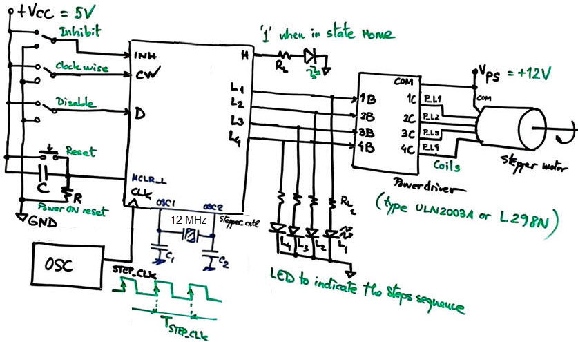
The idea is to connect four outputs to the motor coils and drive them with the right sequence so that the motor inhibits or rotates clockwise or counter-clockwise accordingly to the input signals INH and CW. We can use LED to visualise the binary sequence applied to the coils.
We can imagine a "disabled" state at which all coils are OFF, when switching D = '1'. The motor is not energised and thus the shaft moves freely to a given initial position before starting the motor rotation control.
The MCLR_L that inicialises the microcontroller program memory, will leave the motor in State10 (home). H (home) output, as in the commercial chip L297N, will be high when the controller is in this initial State10.
 |
|
Fig. 2. Symbol and power driver inverter ULN2003A with COM = VPS. In this way, energising a coil (ON), for instance the phase 1, requires L1 = '1', P_L1 = P1' = '0'. |
2. Planning
Design phase #1: basic features. FSM architecture, asynchronous reset (CD_L or MCLR_L), µC quartz crystal oscillator (OSC, 12 MHz), timing diagram, using interrupts, writing outputs, RAM variables, state diagram. Solve the circuit for the design step #1. This means covering P9 and P10 circuits, concepts and ideas. Study, copy and adapt from examples in LAB10.
Project location:
C:\CSD\P10\Stepper_cntl\(files)
- Design step #1: continuous clockwise rotation with external CLK oscillator to fix the rotation speed, and switch D to de-energise the coils to allow the motor shaft move freely.
Modify the Fig. 2 so that it contain only what is necessary to consider in the step #1.
 |
|
Fig. 3. Basic circuit for step #1. |
Adapt the state diagram from D2.2 to this problem. Deduce which signals will be read (in any in this step) and which will generate interrupts.
 |
|
Fig. 4. State diagram adaptation. |
List the required RAM variables and their type. These variables are used as control signals and outputs in the state diagram in Fig. 4.
 |
|
Fig. 5. RAM variables list. |
Draw an example of timing diagram.
 |
|
Fig. 6. Timing diagram example. |
A) Planning hardware
Draw the hardware schematic. Switch P and push-button PB and pull-up resistors, LED to represent the CNTL vector. Reset circuit MCLR_L and a 12 MHz quartz crystal oscillator. External CLK oscillator block. Which pins will interrupt? Which will be read? Assign inputs and outputs to μC port pins.
 |
|
Fig. 7. Hardware used in this application. |
B) Planning software
Draw the software flowchart organised as a FSM.
 |
|
Fig. 8. Software organisation and the idea of FSM adaptation. |
Draw the hardware/software diagram explaining how the FSM is solved in software.
 |
|
Fig. 9. Hardware-software diagram. |
Draw the main ideas of init_system(). Configure input and output pins. Consider as well interrupt configuration bits to enable external interrupts.
 |
|
Fig. 10. TRIS configuration bits. |
Draw the flowchart, memory diagrams and C instructions of read_inputs() function to poll input voltages as in P9.
 |
|
Fig. 11. How to read inputs. |
Draw the flowchart, memory diagrams and C instructions of write_outputs() function to write pin voltages as in P9. At this step the outputs are H and L(4..1.
 |
|
Fig. 12. How to write outputs. |
Infer how to organise the interrupt service routine ISR() to handle push-button falling edge events.
 |
|
Fig. 13. Interrupt service routine flowchart. |
And now, it is necessary to discuss how to transfer all the state transitions into a truth table.
Draw state_logic() truth table and its equivalent flowchart.
 |
Fig. 14. Truth table for state_logic() function and its equivalent behavioural plan B flowchart. |
Draw output_logic() truth table and its equivalent flowchart.
 |
Fig. 15. Truth table for output_logic() function and its equivalent behavioural plan B flowchart. |
3. Development & 4. Test
Develop and test (debugging) the project capturing the hardware circuit in Proteus and writing the C source code. Do not start your hardware circuit and software source file from scratch, but copy and adapt from examples in LAB10 or P10.
- Design step #2. Add the inhibit (INH) and also the CW control signals to the basic FSM.
Go ahead with the step #2 only when step #1 is fully tested working correctly and its report is written. Explain how the new symbol will look like.
Explain what is modified or new in each project section and develop and debug the project.
Design phase #2: advanced features to interface an LCD display.
Add an LCD will indicate ASCII and numerical messages about the motor operation.
Enhance the schematic from design phase #1 to include an LCD attached to port D as studied in tutorials.
Enhance the software and the source file to drive the LCD.
Project location:
C:\CSD\P11\Stepper_cntl_LCD\(files)
In this design phase also two design steps may be conceived, for instance:
- step #1: Print ASCII messages on the LCD.
- step #2: Print as well the rotation speed calculated from the CLK.
Design phase #3: On the use of internal peripherals to reduce components and board size.
The external CLK oscillator circuit will be replaced by internal peripherals TMR2. In this way, we will save power consumption, reduce board footprint, and also free an external INT for other future applications.
Replace the external CLK configuring TMR2 to obtain the same 96 Hz step frequency.
Project location:
C:\CSD\P12\Stepper_cntl_LCD_TMR2\(files)
You can add other features, for instance, if the motor is INH for more than two minutes, a sound signal 2 kHz for a buzzer will be triggered.


