|
|
Bachelor's Degree in Telecommunications Systems and in Network Engineering |
|
Chapter 2 problems |
- D2.6 - |
Serial 8-bit multiplier |
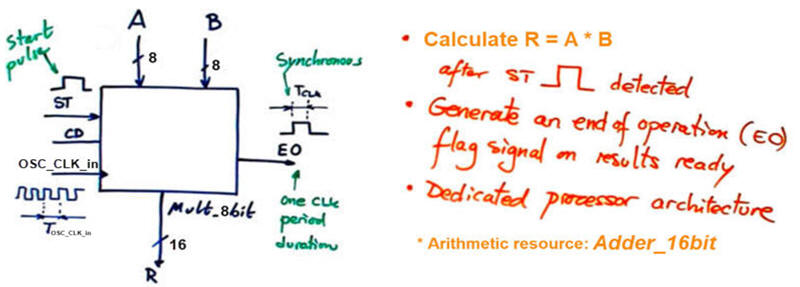
1. Specifications
Design a serial 8-bit multiplier using the algorithm add & shift as proposed in tutorial Mult_4bit. The only arithmetic hardware circuit to use will be an Adder_16bit.
A project on the design of a simple calculator is proposed in D3.6 programming a μC.
The symbol of the circuit is presented in Fig. 1. We will derive a SYS_CLK from the external quartz crystal oscillator to run operations.
 |
| Example timing diagram. |
The idea of multiplying using the shift and add algorithm.
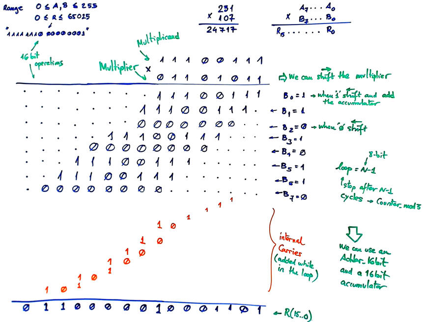 |
| We can multiply in binary radix-2 using the same algorithm we used in primary school. However, this time we better add internal carries along with partial results using the Adder_16bit in every loop cycle. |
Draw an example of operation using the Adder_16bit. Do it in a way that the sequence of basic operations, the algorithm involved in the calculation, is clearly visualised in a way that you can also easily infer the number and type of datapath resources required.
|
|
| Example operation using the Adder_16bit. |
Propose a datapath schematic using components from our products archive.
|
|
Proposed datapath. |
Propose an state diagram for the FSM.
|
|
Proposed state diagram for the FSM. |
Deduce how many D_FF are required when encoding FSM states using the following options and draw the state register memory:
Option #1: radix-2 (sequential)
Option #2: Gray
Option #3: Johnson
Option #4: one-hot
Start a Quartus Prime synthesis project for one of the following programmable target chips:
Option #1: Cyclone IV EP4CE115F29C7
Option #2: MAX II EPM2210F324C3
Option #3: MAX 10 10M50DAF484C7
Draw the testbench fixture.
|
|
| Testbench fixture. |
Calculate the circuit's maximum speed.
|
|
| Timing analyser results to deduce the maximum theoretical operational speed = ___ Mops |
Design the CLK generator circuit from a 50 MHz quartz crystal oscillator to obtain the SYS_CLK signal required to drive the dedicated processor. Deduce the number of D_FF that it will contain.
Option #1: SYS_CLK = 55 kHz
Option #2: SYS_CLK = 22 kHz
Option #3: SYS_CLK = 752 Hz
Optional. Build a prototype for the DE10-Lite board assigning pins and uploading the configuration file to the FPGA.
| Home Term 26/27-Q1 Contact Products Electronic devices and companies Software Books Magazines Instruments DEE Library EETAC DEEL |

|
|
| Web activa des de 09/2001, @ F. J. Robert, Web editat amb Microsoft Expression Web 4. El contingut és un complement als materials d'estudi del curs Circuits i Sistemes Digitals disponibles al campus digital Atenea. Llicència:Reconeixement 4.0 Internacional de Creative Commons |