|
|
Bachelor's Degree in Telecommunications Systems and in Network Engineering |
|
|
|
|||
|
|
Adder_8bit. Plan C2: structural hierarchical multiple-file VHDL |
||
|
|
|||
8-bit radix-2 adder Component and signals
| 1. Specifications | Planning | Developing | Testing | Report | Prototype |
Using VHDL design plan C2, invent an 8-bit binary adder (Adder_8bit) based on simpler chips of the same kind like 4-bit (Adder_4bit) and 1-bit (Adder_1bit) adders. Synthesise it for a target CPLD/FPGA device and test it using VHDL EDA tools.
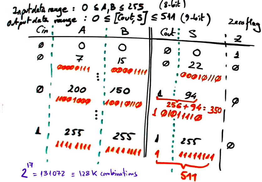
Circuit symbol is represented in Fig. 1 along with its truth table and a sketch of timing diagram.
| |
Fig. 1. a) Symbol of an 8-bit binary adder Adder_8bit (Visio). This is a project Adder_8bit in Proteus. Run it for several input vectors and visualise output results. Examine the commercial chip 74HCT283. |
 |
|
| b) Adder_8bit truth table example values. |
|
 |
|
|
c) Timing diagram sketch showing how
the Adder_8bit performs several
8-bit additions. It is ready for translation as a VHDL
testbench stimulus process. |
|
| Specifications | 2. Planning | Developing | Testing | Report | Prototype |
Plan C2 design flow. Fig 2 shows the proposed architecture for the Adder_8bit, where several components are interconnected rippling carry signals. Logic gates are also used to implement Z output.
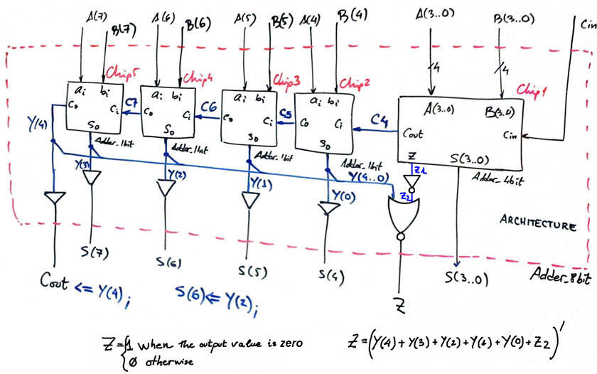 |
Fig. 2. Planning the circuit using several components of the same kind. The carry signal ripples from one component to the next as we do we applying the typical adding algorithm. Output Z is a zero detector that is set only when the 9-bit result is zero. |
Project location:
C:\CSD\P3\Adder_8bit\(files)
| Specifications | Planning | 3. Developing | Testing | Report | Prototype |
We can complete the project Adder_8bit translating the plan C2 schematic in Fig. 2 in this way: "Adder_8bit.vhd".
Before developing this plan, we must copy component VHDL files from other tutorials (see annex below) and paste them in the project's folder.
Run the EDA tool to synthesise the circuit for a given CPLD or FPGA chip. Remember that all the component files have to be also included in the same hierarchical project.
 |
| Fig. 3. Files included in this structure. |
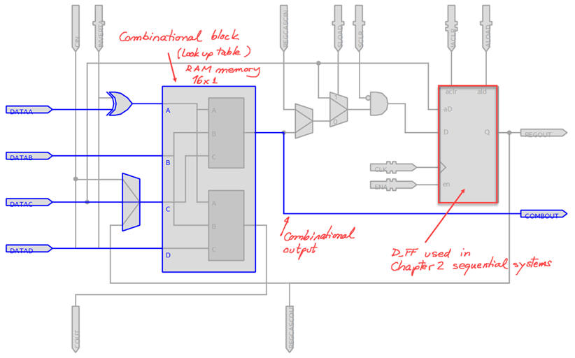
Print and comment the RTL schematic.
 |
| Fig. 4. Example of RTL diagram schematic interpreted by the EDA synthesis tool. |
Print and comment the technology schematic. How many resources (logic cells) are used?
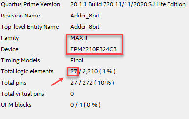 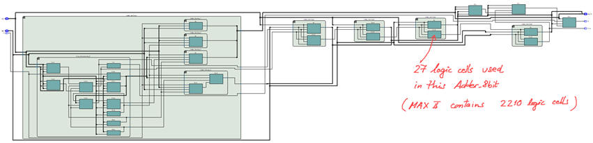 |
| Fig. 5. Example of technology implementation in MAXII CPLD. 27 logic elements are required. |
Quartus Primer Chip Planner tool can be used to pinpoint exactly where the synthesised circuit is placed in the chip fabric.
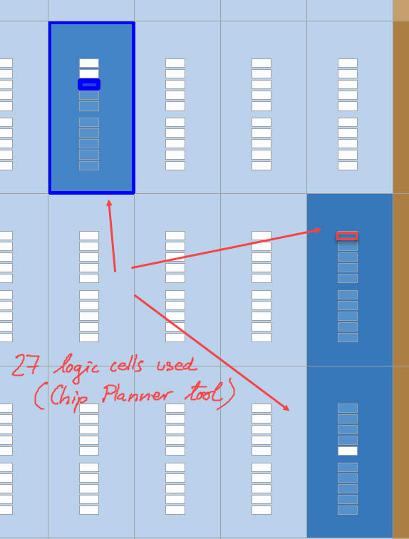  |
| Fig. 6. Quartus Prime tool Chip Planner allows to observe the exact location in the chip where the logic is implemented. As it happens in all our Chapter 1 combinational circuits, the synthesis of truth tables requires only the look-up table (LUT) blocks of the FPGA logic cells. |
| Specifications | Planning | Developing | 4. Testing | Report | Prototype |
Draw the testbench fixture containing the main ideas and concepts involved in this schematic as shown in Fig. 7.
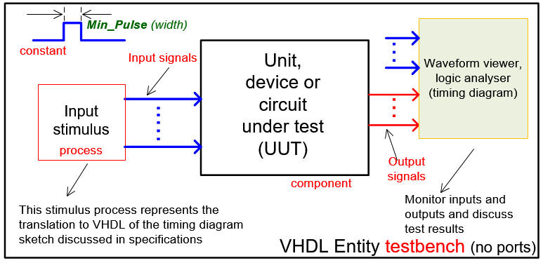 |
| Fig. 7. Testbench VHDL fixture schematic for performing functional and gate-level tests. |
Generate the template of the testbench in Quartus Prime. This is translating into VHDL the schematic in Fig. 7. Rename it and move it to the project folder. Delete the empty process.
Translate the stimulus signals into a process and set the constant Min_Pulse in Fig. 1c. This is a VHDL testbench example file "Adder_8bit_tb.vhd" from which you can copy only the stimulus process and Min_Pulse constant.
Start an EDA VHDL functional simulation project to verify the device-under-test (DUT) using the test bench.
Run simulations and demonstrate how the circuit works adding handwritten comments to the printed sheet of paper containing the waveforms. Vertical cursors are required to separate the different truth table combinations under test.
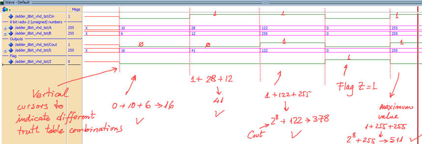 |
| Fig. 8. Analysing results from functional simulation of the Adder_8bit. |
| Specifications | Planning | Developing | Testing | 5. Report | Prototype |
It is required a handwritten original project report containing sections 1 - 2 - 3 - 4, scanned figures with annotations, file listings, diagrams, sketches or any other resources. Theory and other materials to comprehend how the circuit works may be included in section 1 on specifications. Annexes be included to describe the components used in the planning.
Follow this rubric for writing reports.
Components used in this Adder_8bit, can be reported as annexes.
The idea of technical report at this level has to be clear for you now: a document that demonstrates the way you have designed a given product. Furthermore, it allows you to prepare an oral presentation because it includes everything to generate slides. Simple class notes and conventional exercises may be right for passing exams, but using your project reports you'll be able to teach your peers as if you had become a class instructor.
| Specifications | Planning | Developing | Testing | Report | 6. Prototype |
Use training boards and perform laboratory measurements to verify how the circuit being designed works for real.
Example 1. Prototyping Adder_8bit circuit using a Terasic DE2-115 FPGA platform.
 |
|
Fig. 8. DE0-115 board representing only simple digital inputs (buttons and switches) and outputs (LED and 7-segments). |
Annexes: Adder_8bit components
Because this design is complex, better if we go step by step bottom-up starting from the most simple component: 1-bit full adder (Adder_1bit) at the same time that we practice plan C2.
Therefore, below is the proposed general organisation to complete our chip Adder_8bit:
Adder_1bit (projects 1 or 2 or 3 or 4) ----> Adder_4bit (projects 5 or 6) ----> Adder_8bit
Annex 1: Adder_1bit projects
To solve this component we present up to four architectures:
Project 1: Let us design the Adder_1bit using plan C2 and the MoM that is explained in L3.3. This is the first project in this lab tutorial.
C:\CSD\P3\Adder_1bit_MoM\(files)
Project 2: Let us design the Adder_1bit using plan C2 and the method of decoders MoD that is explained in L3.3.
C:\CSD\P3\Adder_1bit_MoD\(files)
Project 3: Let us design the Adder_1bit using plan A.
C:\CSD\P3\Adder_1bitA\(files)
Project 4: Let us design the Adder_1bit using plan B.
C:\CSD\P3\Adder_1bitB\(files)
Annex 2: Adder_4bit projects
To solve this component we present two architectures that will have different performance when implemented in a given CPLD chip.
Project 5: Let us design a ripple carry Adder_4bit.
C:\CSD\P3\Adder_4bit_RC\(files)
Project 6: Let us design a carry-lookahead Adder_4bit. This design is similar to the standard chip type 74HCT283.
C:\CSD\P3\Adder_4bit_CLA\(files)
Note: This CLA 4-bit adder version includes two extra outputs (P, G) that may be left unconnected modifying the top schematic in this way: Adder_8bit.vhd.
Optional supplemental resources
This is another version of Adder_8bit using plan B. We simply describe inputs, outputs and the behaviour of the high-level algorithm. EDA tools will synthesise the best and optimised circuit considering the target FPGA.
| Home Term 26/27-Q1 Contact Products Electronic devices and companies Software Books Magazines Instruments DEE Library EETAC DEEL |

|
|
| Web activa des de 09/2001, @ F. J. Robert, Web editat amb Microsoft Expression Web 4. El contingut és un complement als materials d'estudi del curs Circuits i Sistemes Digitals disponibles al campus digital Atenea. Llicència:Reconeixement 4.0 Internacional de Creative Commons |