|
|
Bachelor's Degree in Telecommunications Systems and in Network Engineering |
|
|
|
Adder_1bit plan C2: structural hierarchical multiple-file VHDL |
MoM for implementing logic functions
| 1. Specifications | Planning | Developing | Functional test | Gate-level test | Prototype | Report |
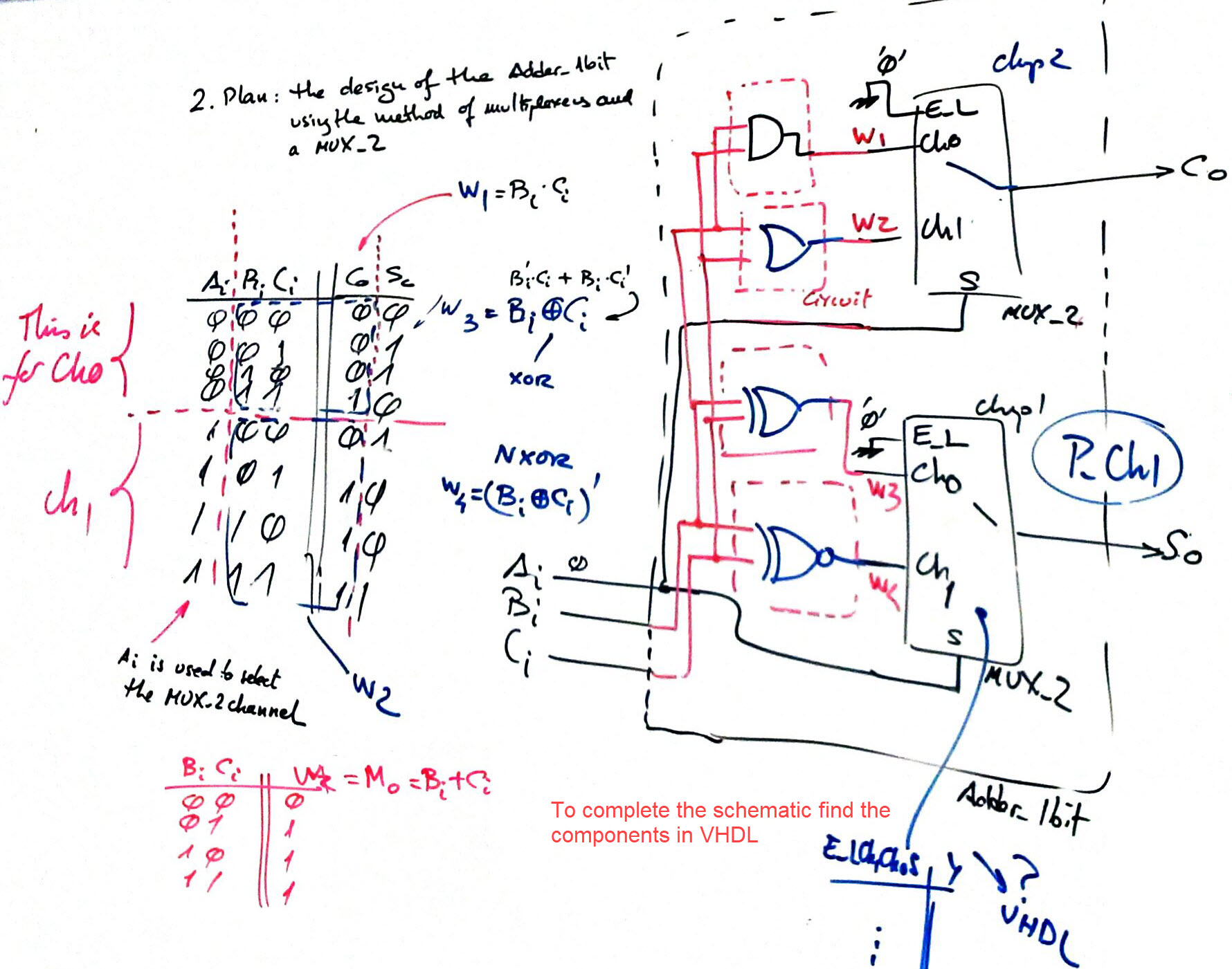
Design a 1-bit adder using plan C2 and the method of multiplexers MoM using a MUX_2 for So and a MUX_4 for Co.
 |
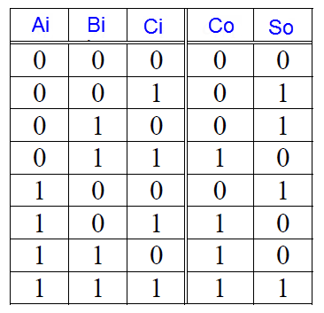 |
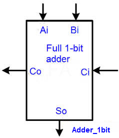
Fig. 1. Symbol and truth table of 1-bit adder circuit (full adder). |
Fig. 2 is a sketch that represents the truth table in time. The idea of applying input vectors that can be any binary combination.
 |
| Fig. 2. Timing diagram where all the inputs are applied sequentially and hence, the output is predicted accordingly to the truth table. |
| Specifications | 2. Planning | Development | Functional test | Gate-level test | Prototype | Report |
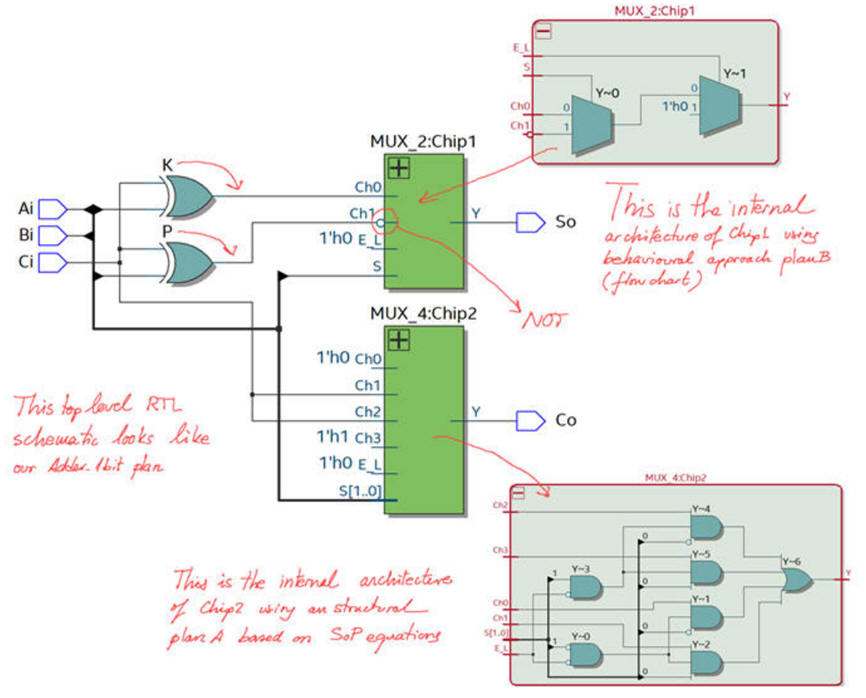
We will conceive all our circuits using VHDL EDA tools and following the design flow. Fig. 3 shows the internal architecture of the Adder_1bit based on the MoM and using specifically a MUX_4 for Co = f(Ai, Bi, Ci) and a MUX_2 for So.
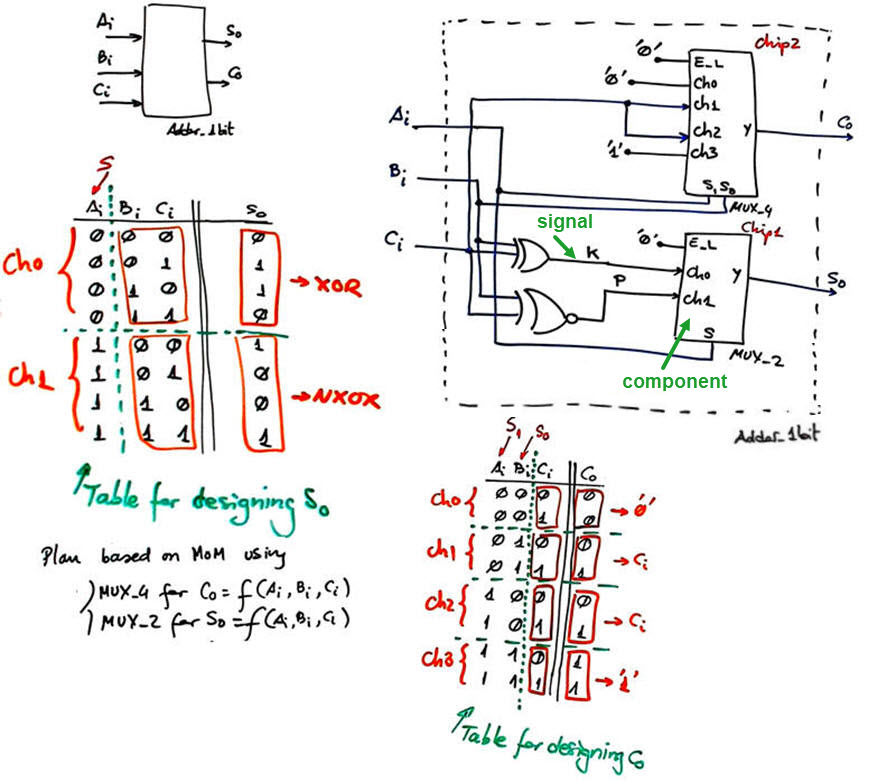 |
| Fig. 3. Plan proposed for this project. The concept of components and signals in a structural hierarchical schematic. |
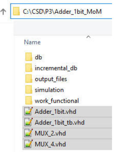
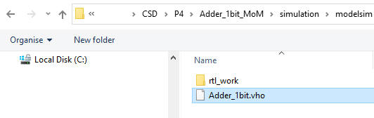
Project location:
C:\CSD\P3\Adder_1bit_MoM\(files)
Alternatively, as a way to generate additional projects using plan C2, we can imagine other similar hierarchical schematics:
(1) Propose a plan using MUX_2 for both outputs.
(2) Propose a plan using MUX_4 for both outputs.
(3) Design the Adder_1bit circuit using a single component MUX_8.
| Specifications | Planning | 3. Development | Functional test | Gate-level test | Prototype | Report |
|
General rule in CSD for saving study time and wasted efforts: NEVER develop (beginning of project section #3) a circuit without a perfect schematic in paper ready for VHDL translation (the end of project section #2). Example schematic not ready Example schematic ready for VHDL |
This "Adder_1bit.vhd" is the translation of the circuit in Fig. 3 above.
The components have their own translation to VHDL, for instance: "MUX_4.vhd" (using plan A adapted from this MUX_8 tutorial in Lab2), "MUX_2.vhd" (using plan B adapted from this tutorial in Lab2).
Implement a new synthesis project using Quartus Prime for a given Intel target chip: FPGA Cyclone IV EP4CE115F29C7.
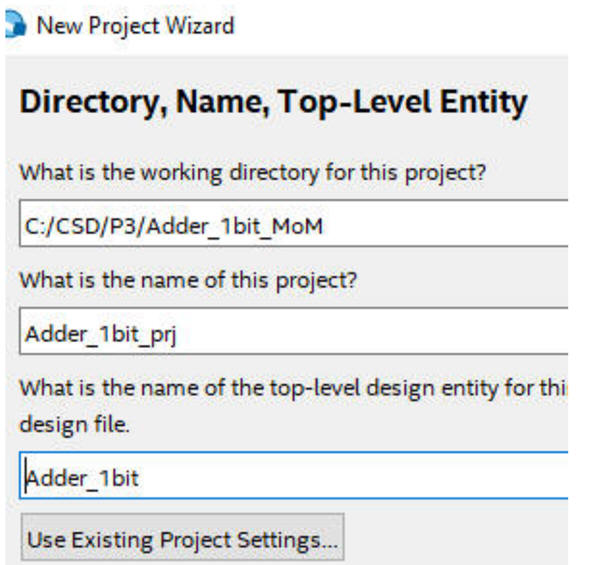 |
| Fig. 4. New project. |
Add all the VHDL files that define the plan C2 architecture before synthesising the project.
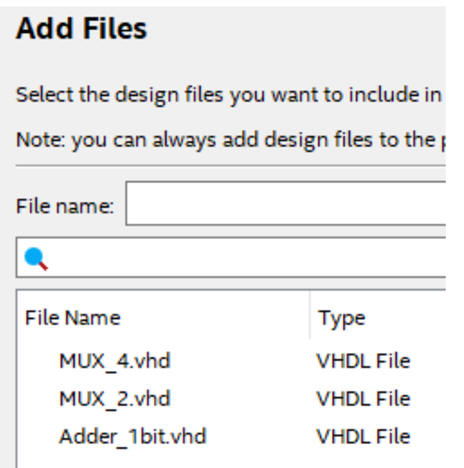 |
| Fig. 5. Adding files. |
Print and discuss RTL and technology circuits.
 |
| Fig. 6. RTL circuit. |
How many chip resources (logic cells) are used? Why technology circuit (the real circuit implemented into the target chip differs from the ideal RTL circuit written in VHDL?
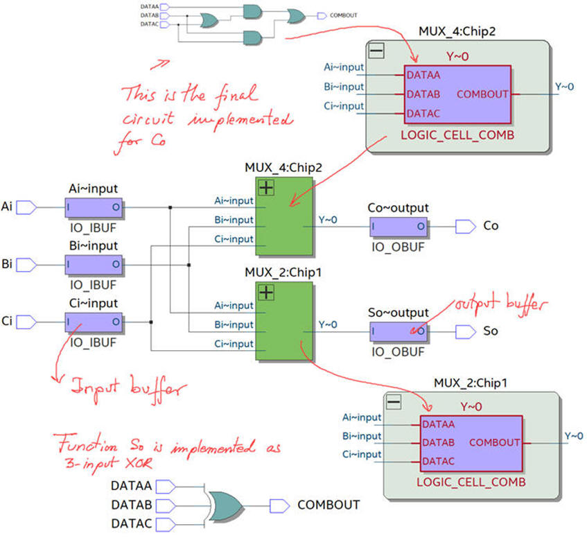 |
| Fig. 7. Technology circuit. |
| Specifications | Planning | Developing | 4. Functional test | Gate-level test | Prototype | Report |
Draw a testbench fixture. We will simulate in ModelSim a VHDL testbench for the unit-under-test.
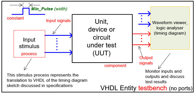 |
| Fig. 8. Testbench VHDL fixture schematic for performing functional and gate-level tests. |
Generate the VHDL skeleton in Quartus Prime. Translate it to a testbench file. This is an example of testbench file "Adder_1bit_tb.vhd" from which you can copy only the stimulus process and the constant Min_Pulse. For instance Min_Pulse = 3.55 ms for referencing time. Remember that from testing point of view, even if you have designed the Adder_1bit using several plans, you can use all the time the same testbench.
Generate a new functional simulation project in ModelSim considering all the structural VHDL files and the top testbench.
 |
| Fig. 9. VHDL structural files. |
Run enough time (for example, run 710 ms = 200*Min_Pulse) and interpret simulation results printing and commenting waveforms.
 |
| Fig. 10. Handwritten comments on the waveforms results. |
| Specifications | Planning | Developing | Functional test | 5. Gate-level test | Prototype | Report |
Two new tools will be presented:
-
(1) ModelSim gate-level simulations for measuring propagation delays in a given signal transition.
-
(2) Quartus Prime timing analyser for calculating the worst-case scenario (longest propagation delay).
The objective is to find what target chip is faster when implementing the same project Adder_1bit:
-
Option #1: MAXII device EPM2210F324C3
-
option #2: Cyclone IV EP4CE115F29C7
Firstly, we will solve the project for chip option #1 and annotate results. Secondly, keeping the same project, we will modify the configuration of the Quartus Prime project to change the target chip to option #2 and annotate results. We will discuss solutions.
We can start a new Quartus Prime project copying the source VHDL files "Adder_1bit.vhd", "MUX_2.vhd", "MUX_4.vhd" and the testbench files "Adder_1bit_tb.vhd", "wave.do" to this new location:
C:\CSD\P4\Adder_1bit_MoM\(files)
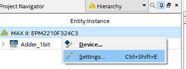
Select the option #1 MAX II target device and synthesise the circuit.
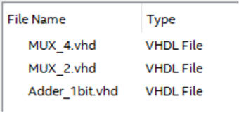 |
Fig. 11. Plan C2 source files. |
Be sure that you check the RTL and technology view as you did in Fig. 6 and Fig. 7.
Check that you've got the same functional test results in Fig. 10 when using the same VHDL testbench fixture "Adder_1bit_tb.vhd". Use the same "wave.do" for setting up the signals of interest in the wave diagram.
Gate-level VHDL simulation of the technology schematic
Let us use the new tools that will allow us to characterise better the real circuit implemented in the FPGA. This is our tutorial on gate-level simulation and the timing analyser tool in case you needed it even before running this tutorial.
Set the following project parameters before re-synthesising your project and be able to generate the necessary VHO and SDO files for the target chip:
 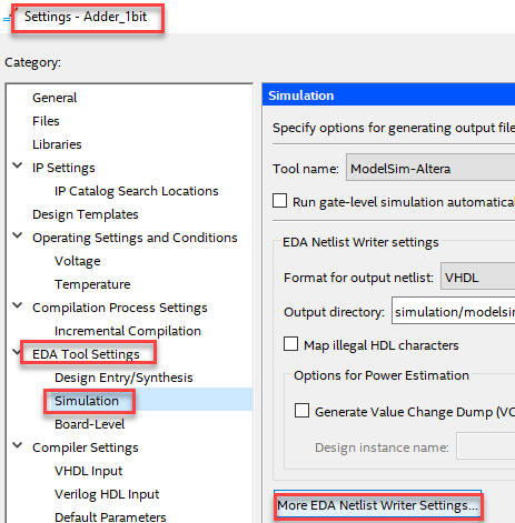 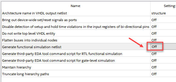 |
| Fig. 12. Parameters for letting Quartus Prime generate delay files. |
And now re-synthesise your project to generate in Quartus Prime the VHDL translation of the technology circuit "Adder_1bit.vho" and its delay file "Adder_1bit_vhd.sdo".
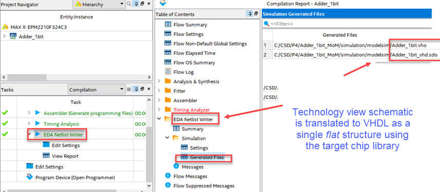 |
| Fig. 13. Indications for generating the VHDL technology circuit translation (vho) along with its delay file (sdo). |
Now you are ready for starting a ModelSim gate-level simulation for this flat circuit.
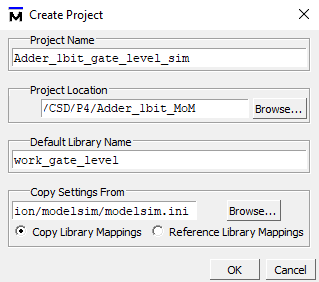 |
| Fig. 14. Create a new ModelSim project. |
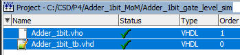
Add the same testbench that you used above in functional simulation to the new location:
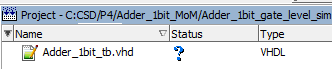  |
| Fig. 15. Add the same testbench and flat structure. |
Compile all and check the project's integrity. Therefore, hierarchical structures formed by multiple VHDL files are replaced by a single flat VHO file to be tested using the same testbench.
 |
| Fig. 16. Check the project integrity. |
Start a new simulation paying attention this time to both "Design" and "SDF" tabs:
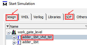 |
| Fig. 17. |
Attach the standard delay file to the region of interest:
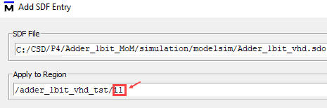 |
| Fig. 18. The region where to apply the SDO file is the instance i1 (the unit-under-test). |
Run and check that the full wave is the same as it was in functional simulations.
 |
| Fig. 19. Full view of the simulation results. |
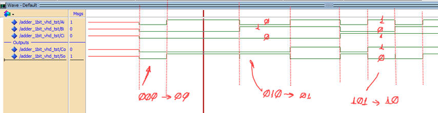
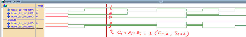
Zoom at a given signal transition to measure propagation delays using two cursors. For instance, zoom the transition from "110" to "001" that implies switching the two outputs.
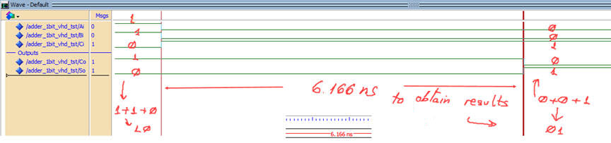 |
| Fig. 20. In this example transition, both outputs changes from "10" to "01" after 6.17 ns. |
Therefore, paying attention to Fig. 20, this is the experiment that we are simulating.
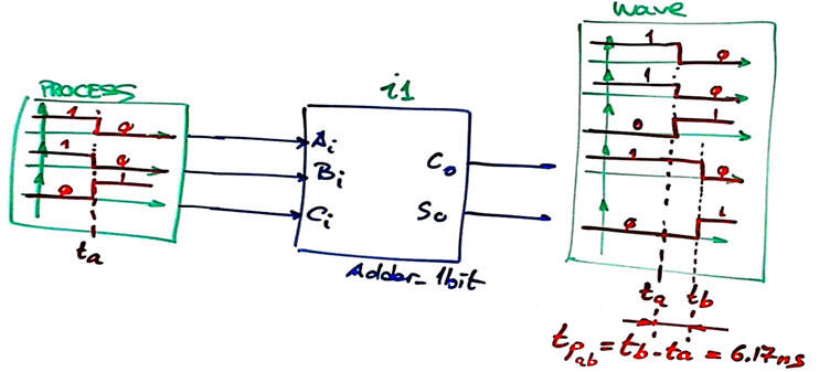 |
| Fig. 21. Schematic representation of the experiment observed in the transition from input combination "110" to "001" where both outputs switch values. |
Timing analyser tool: longest propagation time tP and maximum speed of operation
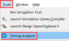
Go back to Quartus Prime to find the largest propagation delay associated to a given signal path from input to output using the timing analyser spreadsheet tool.
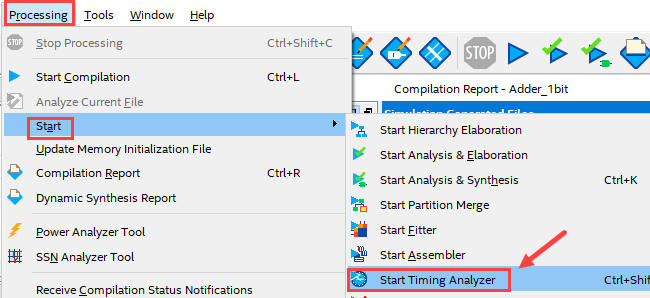 |
| Fig. 22. Starting processing the timing analyser tool. |
View results in the spreadsheet.
 |
| Fig. 23. View results using the timing analyser tool. |
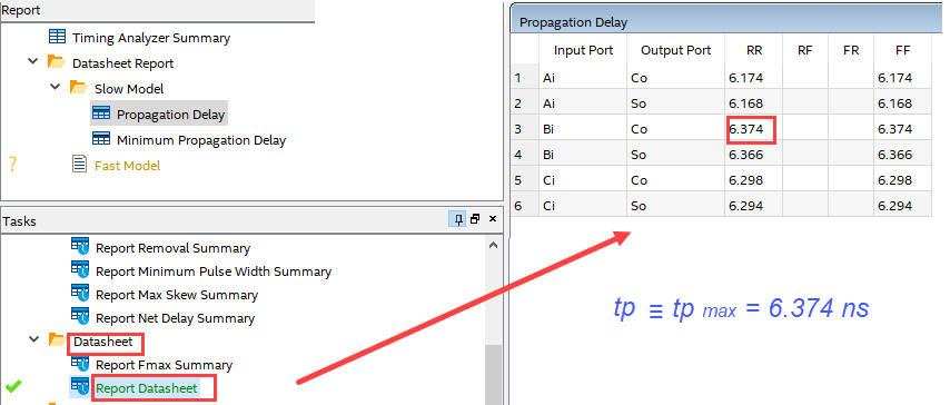 |
| Fig. 24. Spreadsheet from datasheet report. |
And so, calculate the maximum frequency of operation for this specific target chip MAX II (L4.3):
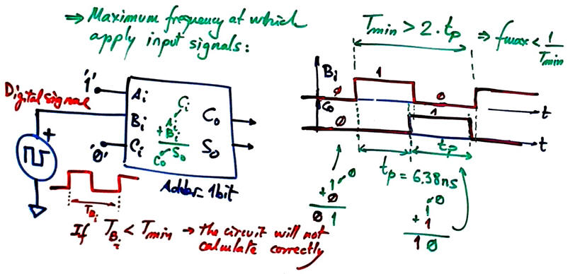  |
| Fig. 25. Maximum generator frequency at which this Adder_1bit can perform. Meaning that the circuit is capable of performing at a theoretical operational speed = 156 Mops (millions of operations per second). |
And now, you can redo the project (at the same location), changing the target chip and compare how this Addder_1bit is performing for an option #2 Cyclone IV target chip.
 |
| Fig. 26. Select a Cyclone IV device FPGA (Field Programmable Gate Array). |
Check that the files of interest are correctly generated for this new target chip. Indeed here you can find several simulation models (fast, slow, etc.):
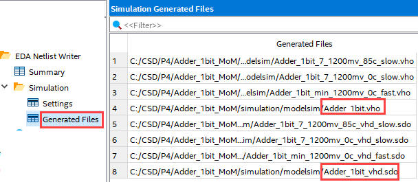 |
| Fig. 27. For this chip several delay models are generated. |
Recompile your ModelSim project and write down results:
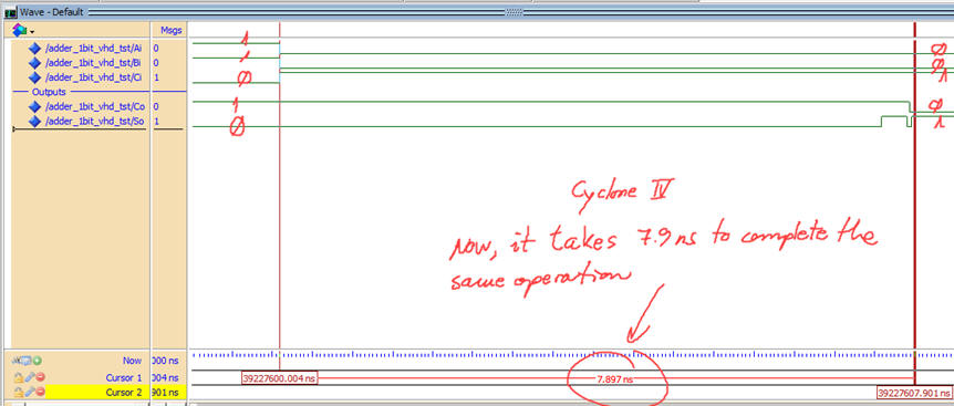 |
| Fig. 28. Cyclone IV measurements are slightly different at the same transition. |
And, using the timing analyser, we can observe a longer propagation delay than in MAX II.
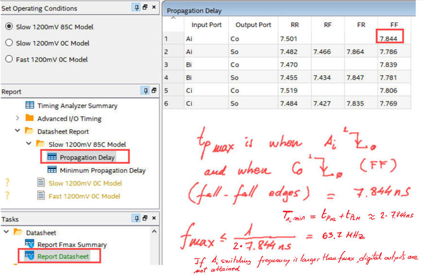 |
| Fig. 29. Cyclone IV measurements are slightly different at the same transition. Thus, for this target chip speed = 127 Mops (millions of operations per second). |
And thus, the theoretical maximum frequency of operation for the target chip Cyclone IV is slower that for the MAXII.
| Specifications | Planning | Developing | Functional test | Gate-level test | 6. Prototype | Report |
A prototype on arithmetic circuits, an ALU_9bit design, is presented in the next LAB4.2.
| Specifications | Planning | Developing | Functional test | Gate-level test | Prototype | 7. Report |
Follow this rubric for writing reports.
| Home Term 26/27-Q1 Contact Products Electronic devices and companies Software Books Magazines Instruments DEE Library EETAC DEEL |

|
|
| Web activa des de 09/2001, @ F. J. Robert, Web editat amb Microsoft Expression Web 4. El contingut és un complement als materials d'estudi del curs Circuits i Sistemes Digitals disponibles al campus digital Atenea. Llicència:Reconeixement 4.0 Internacional de Creative Commons |