|
|
Bachelor's Degree in Telecommunications Systems and in Network Engineering |
|
Chapter 2 problems |
- D2.13 - |
Serial 20-bit adder (FPGA-VHDL) |
1. Specifications
Design a 20-bit serial adder using the algorithm add & shift as proposed in tutorial Adder_4bit. The only arithmetic hardware circuit to use will be an Adder_3bit. Planning will be based on a dedicated processor architecture.
A project on the design of a simple calculator is proposed in D3.6 programming a μC.
The symbol of the circuit is presented in Fig. 1. We will derive a SYS_CLK from the external quartz crystal oscillator to run operations.
 |
| Fig. 1. Symbol for the barrel 3_shift register of 21-bit required in this project. |
 |
| Fig. 2. Example timing diagram. |
The idea of adding algorithm using limited resources. We need to shift and add partial results to obtain after several iterations the final result.
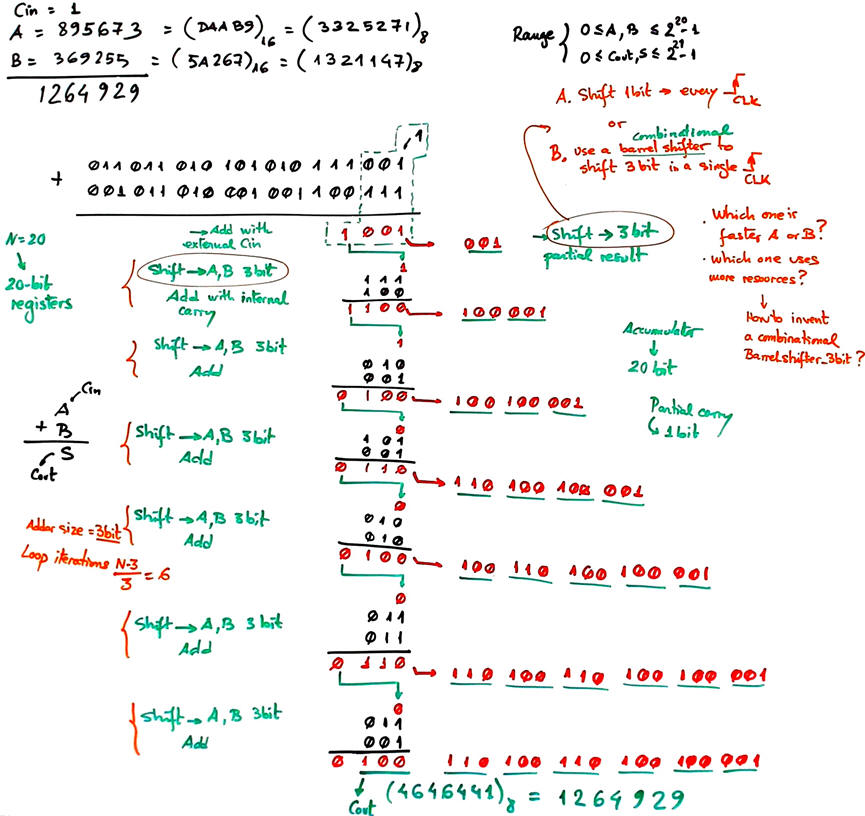 |
| Fig. 3. The idea of adding using limited arithmetic resources. |
From this example we see that the key operation repeated multiple times is the 3-bit right shifting. Hence, a typical Shift_reg_nbit component may not be that useful because it will imply shifting 20 bits one by one and the size of the adder (Adder_3bit) will not offer any advantage with respect to the simpler Adder_1bit.
Therefore, we better invent a 21-bit barrel shift register, a device capable of shifting 3-bit in a single CLK period. We can add synchronicity and parallel load capabilities to this device converting it in a generalised barrel 3_shift register. The assignment D1.9 shows the combinational version of this component.
We will study this barrel p_shift register of n-bit project in this lecture L7.2 as another example on registers. You will find its VHDL translation Barrel_3_shift_reg_21bit product. This device offers some flexibility and it can be used as well as a simple 21-bit data register.
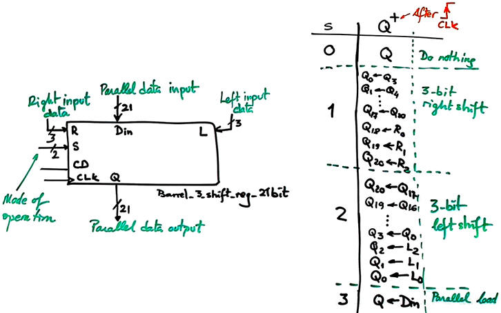 |
| Fig. 4. Symbol for the barrel 3_shift register of 21-bit required in this project. |
Draw an example of flowchart to visualise the sequence of operations or the algorithm involved in the calculation. Try several similar operations as in Fig. 3.
|
|
| Fig. 5. Example operation using the Adder_3bit. |
Propose a datapath as represented in Fig. 6. Check its feasibility or add convenient modifications.
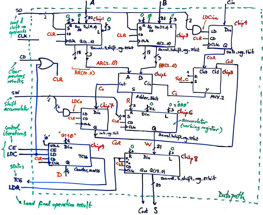 |
Fig. 6. Imagining a possible operational unit (datapath) adapting the tutorial Adder_4bit. |
Propose an state diagram for the FSM.
|
|
Proposed state diagram for the FSM. |
|
|
Schematic of the dedicated processor. |
Deduce how many D_FF are required when encoding FSM states using the following options and draw the state register memory:
Option #1: radix-2 (sequential)
Option #2: Gray
Option #3: Johnson
Option #4: one-hot
Start a Quartus Prime synthesis project for one of the following programmable target chips:
Option #1: Cyclone IV EP4CE115F29C7
Option #2: MAX II EPM2210F324C3
Option #3: MAX 10 10M50DAF484C7
Draw the testbench fixture.
|
|
| Testbench fixture. |
Calculate the circuit's maximum speed.
|
|
| Timing analyser results to deduce the maximum theoretical operational speed = ___ Mops |
Design the CLK generator circuit from a 50 MHz quartz crystal oscillator to obtain the SYS_CLK signal required to drive the dedicated processor. Deduce the number of D_FF that it will contain.
Option #1: SYS_CLK = 75 kHz
Option #2: SYS_CLK = 33 kHz
Option #3: SYS_CLK = 1.45 kHz
Optional. Build a prototype for the DE10-Lite board assigning pins and uploading the configuration file to the FPGA.
| Home Term 26/27-Q1 Contact Products Electronic devices and companies Software Books Magazines Instruments DEE Library EETAC DEEL |

|
|
| Web activa des de 09/2001, @ F. J. Robert, Web editat amb Microsoft Expression Web 4. El contingut és un complement als materials d'estudi del curs Circuits i Sistemes Digitals disponibles al campus digital Atenea. Llicència:Reconeixement 4.0 Internacional de Creative Commons |