|
|
Bachelor's Degree in Telecommunications Systems and in Network Engineering |
|
|
|
|||
|
|
(A) 4-bit serial adder |
(B) 20-bit serial adder |
|
|
|
|||
Dedicated processor (datapath + control unit)
| 1. Specifications | Planning | Developing | Test functional | Test gate-level | Prototype | Report |
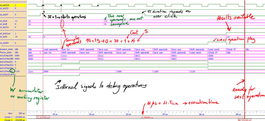
Let us propose another version of the Adder_4bit. This time it will be a sequential system organised as a dedicated processor. The symbol is proposed in Fig. 1. The device will sample A, B and Cin operands after detecting the start (ST) click. The operation will run for several CLK cycles and when the result (Cout, S) ready an end of operation flag (EO) pulse will the asserted, thus the machine will be ready to perform another operation. We will derive an internal system CLK (SYS_CLK) from the external quartz crystal oscillator to run operations.
The idea of such serial adder is to perform large calculations using limited arithmetic hardware resources. In this case, simply a 4-bit addition using only one Adder_1bit. Another similar full tutorial shows how to create a Mult_8bit using only one Adder_16bit. And even another one shows a typical add-and-accumulate algorithm. Similar approaches can be taken for example when performing 64-bit arithmetic operations in 8-bit microprocessor hardware.
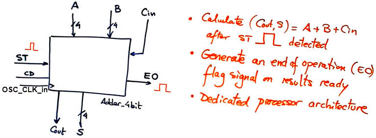 |
| Fig. 1. Symbol. |
Fig. 2 shows an example addition: 6 + 14 + 1 = 21. The operating time takes several CLK periods. Input data can be changes any time, only the values sampled after the ST pulse will be processed. In the same way, another ST click while operating will be ignored. Results will be kept available until the next operation.
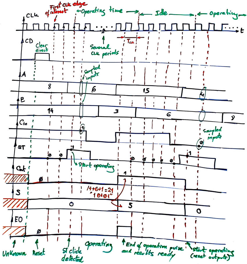 |
| Fig. 2. Example timing diagram. |
The duration of the start pulse must be taken into account so that when too long, the processor will not start a new operation, it will stop waiting for the signal go down.
Alternatively, as a better solution to handle user clicks, we can use a synchroniser to generate TCLK duration ST pulses for activating the processor. This extra circuit (hardware) will shorten and make more robust and reliable the state diagram (software).This is the way to introduce as well in the design of the dedicated processor the CLK_Generator component (L8.2) to obtain all the required CLK signals to run the machine, for instance 200 Hz for the button interface, 10 MHz for the processor.
Let us synthesise the project for the MAX10 FPGA building a prototype on the DE10-Lite board.
Additional circuits may be included in the top design to be able to represent results in BCD lighting 7-segment digits.
In the same way, additional adaptation circuits may be added to the basic design to operate with integer numbers for adding and subtracting in 2C.
Notes from a book on an example design and the idea of the add and shift algorithm.
| Specifications | 2. Planning | Developing | Test functional | Test gate-level | Prototype | Report |
Devise a top schematic based on organising a dedicated processor architecture as in Fig. 3 that suit almost any application.
 |
| Fig. 3. Dedicated processor concept. |
The design starts imagining the data and the arithmetic and logic operations involved in the add and shift algorithm.
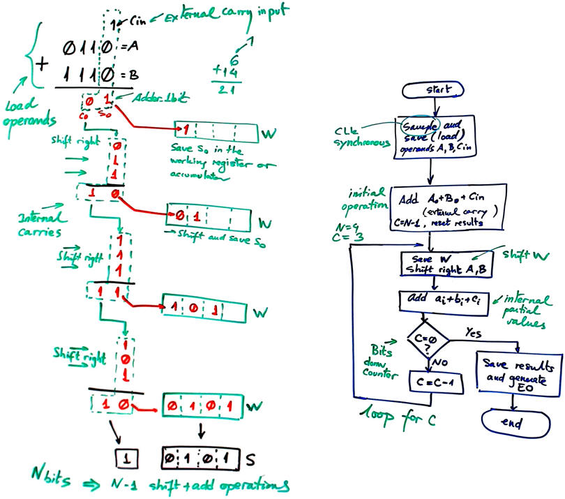 |
| Fig. 4. Example operation using the Adder_1bit. As shown in the approximate algorithm represented as a flowchart (pseudo-code), data and shift registers are required to save partial sums and carries. |
The datapath will be in charge of operating the algorithm, and we can imagine how many components will be included and how to connect them so that operands can be shifted and conveyed to the single Adder_1bit available while saving partial and final data. We propose to use standard components, such Shift_reg_4bit for all memory registers or Counter_mod16 for controlling the shit and add loop. The synthesiser will optimise the number of resources used.
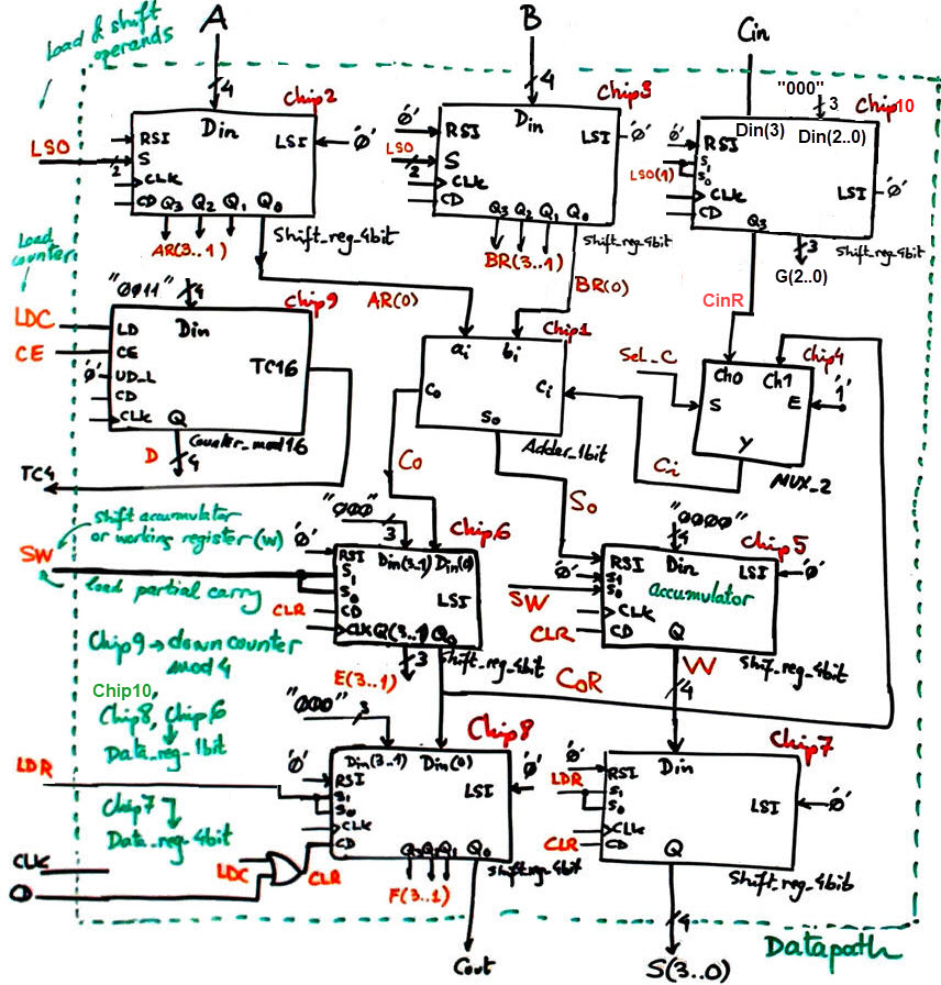 |
| Fig. 5. Proposed datapath using multiple times the same Shift_reg_4bit for both data register and shifter. |
Number of registers used in this application datapath:
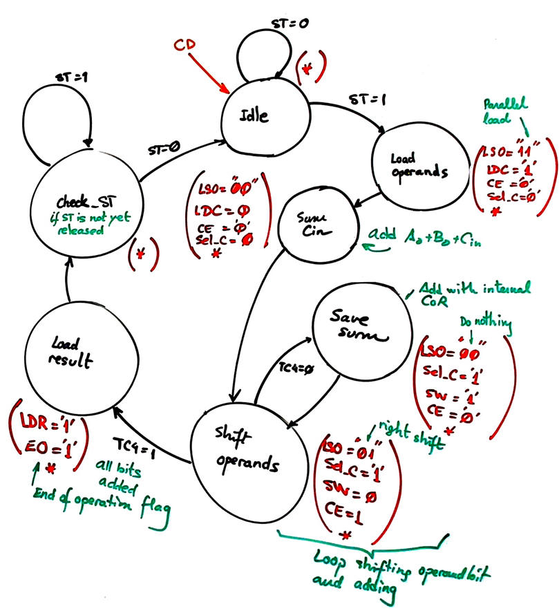
The control unit FSM will generate all the datapath control signals and activate them in the corresponding states. Fig. 6 shows an example of state diagram. The processor will be idle until ST is sample high, the first operation will be considering the external Cin, the other three in a loop will include the internal carry signal CoR.
 |
| Fig. 6. Control unit state diagram. |
In this way, the top dedicated architecture adapted to solve this project will be as represented in Fig. 7 adding the CLK_Generator circuit to obtain the SYS_CLK with the frequency given as a design option.
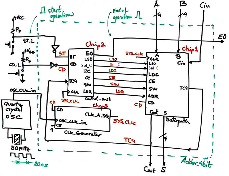 |
| Fig. 7. Top dedicated processor system. |
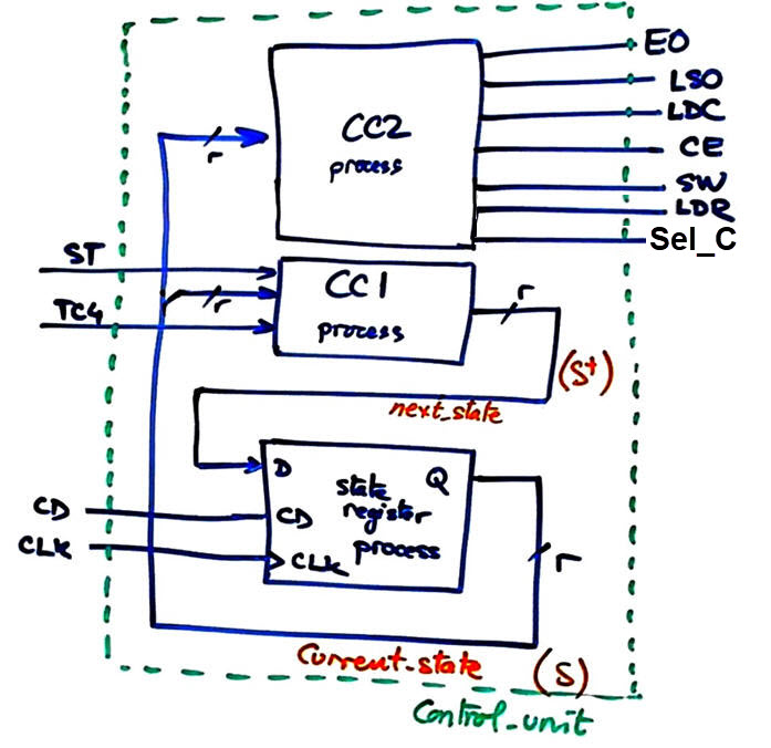
The control unit will be a FSM as proposed in L6.1. Adapt its general architecture to this problem explaining where each signal is connected.
 |
| Fig. 8. FSM for this project. It is translated as a single plan C1 circuit into VHDL using behavioural descriptions. |
Deduce how many D_FF are required when encoding FSM states using the following options and draw the state register memory:
Option #1: radix-2 (sequential). 7 states means that r = 3 , and one code is never used.
Option #2: Gray. 7 states means that r = 3 , and one code is never used.
Option #3: Johnson. 7 states means that r = 7
Option #4: One-hot. 7 states means that r = 7
Draw the FSM CC2 truth table and their equivalent behavioural interpretations (plan B) using flowcharts ready for VHDL translation.
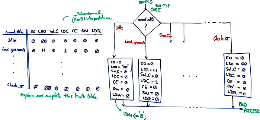 |
| Fig. 8. CC2 truth table and flowchart. |
Draw the FSM CC1 truth table and flowchart ready for VHDL translation.
 |
| Fig. 9. CC1 truth table and flowchart. |
Project location:
C:\CSD\P8\Adder_4bit\(files)
| Specifications | Planning | 3. Developing | Test functional | Test gate-level | Prototype | Report |
Write the VHDL files to translate your plans. Find in our products portfolio the required components. Components not available will be designed from similar ones and reported as an annex.
File list:
Start a Quartus Prime synthesis project for one of the following programmable target chips:
Option #1: Cyclone IV EP4CE115F29C7
Option #2: MAX II EPM2210F324C3
Option #3: MAX 10 10M50DAF484C7
Check the resources used, specially the number of D_FF.
 |
| Fig. 10. Resource used. |
Inspect and discuss your RTL view schematic.
|
|
| Fig. 11. RTL. |
Technology view and resources located in the Chip Planner.
|
|
| Fig. 12. Technology |
All the "Adder_4bit.zip" project files.
| Specifications | Planning | Developing | 4. Test functional | Test gate-level | Prototype | Report |
Testbench fixture.
|
|
| Fig. 13. Testbench fixture. |
|
|
|
| Fig. 14. Testing. | |
| Specifications | Planning | Developing | Test functional | 5. Test gate-level | Prototype | Report |
We can try to measure the circuit's theoretical maximum frequency of operation replacing only for this measurement the MAX10 FPGA by a Cyclone IV or a MAXII device.
|
|
| Fig. 15. Timing analyser results to deduce the maximum theoretical operational speed = ___ Mops |
| Specifications | Planning | Developing | Test functional | Test gate-level | 6. Prototype | Report |
We can imagine the Adder_4bit adapted to a matrix keypad (P6) and to 7-segment displays (P2) for inputting operands and visualising results.
| Specifications | Planning | Developing | Test functional | Test gate-level | Prototype | 7. Report |
Follow this rubric for writing reports.
|
|
(A) 4-bit serial adder |
(B) 20-bit serial adder |
| 1. Specifications | Planning | Developing | Test functional | Test gate-level | Prototype | Report |
Solve this variation for the same serial adder concept.
 |
| Fig. 1. Initial sketch representing the circuit symbol. |
| Home Term 26/27-Q1 Contact Products Electronic devices and companies Software Books Magazines Instruments DEE Library EETAC DEEL |

|
|
| Web activa des de 09/2001, @ F. J. Robert, Web editat amb Microsoft Expression Web 4. El contingut és un complement als materials d'estudi del curs Circuits i Sistemes Digitals disponibles al campus digital Atenea. Llicència:Reconeixement 4.0 Internacional de Creative Commons |