|
|
Bachelor's Degree in Telecommunications Systems and in Network Engineering |
|
Chapter 2 problems |
- D2.12 - |
Electronic roulette (FPGA-VHDL) |
1. Specifications
Let us design an electronic roulette as shown in Fig. 1. After turning on the power supply, a 3.3 V battery, the roulette inicialises showing number 0 (yellow LED). While the user is clicking and holding the play (P_L) button the LED wheel is spinning and when the button P_L is released a new bet is shown. The circuit keeps the last bet LED lighting.
Let us invent this circuit using plan C2 and proposing a dedicated processor 8.1 architecture for controlling the play button and counting a random number.
The same project designed programming a μC is in D3.12.
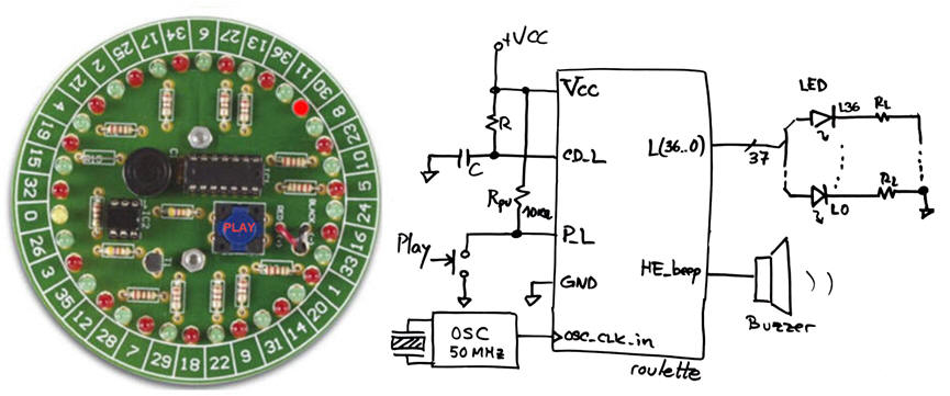 |
| Fig. 1. Electronic roulette. The wheel have a zero (house edge), and numbers from 1 to 36. The odds of winning a bet for a single number are thus thirty seven to one (2.7%). |
Fig. 1 shows the symbol of the top schematic Roulette. Now it is time to imagine how the circuit may work in time as an standard Chapter 2 circuit, with button detection and code generation.
Sketch a timing diagram showing how the circuit operates. The Fig. 2 is a first example. We assume option CLK #1 values, we imagine that in a first design the LED spin at the same frequency for generating a random number.
 |
| Fig. 2. Example of initial timing diagram. While betting the one-hot numbers (only one LED lighting at a time and rotating) are generated at a large weird frequency. To start the project, and because the CLK_generator for the one-hot code is not yet designed, we can imagine that the numbers are also generated at the frequency Sys_CLK used for sampling the play button. |
From these preliminary ideas, the project continues planning the Datapath, the CLK_Generator and the FSM components for the dedicated processor.
2. Planning
Design phase #1: Basic features: step #1: FSM, step #2: datapath and step #3: CLK_Generator
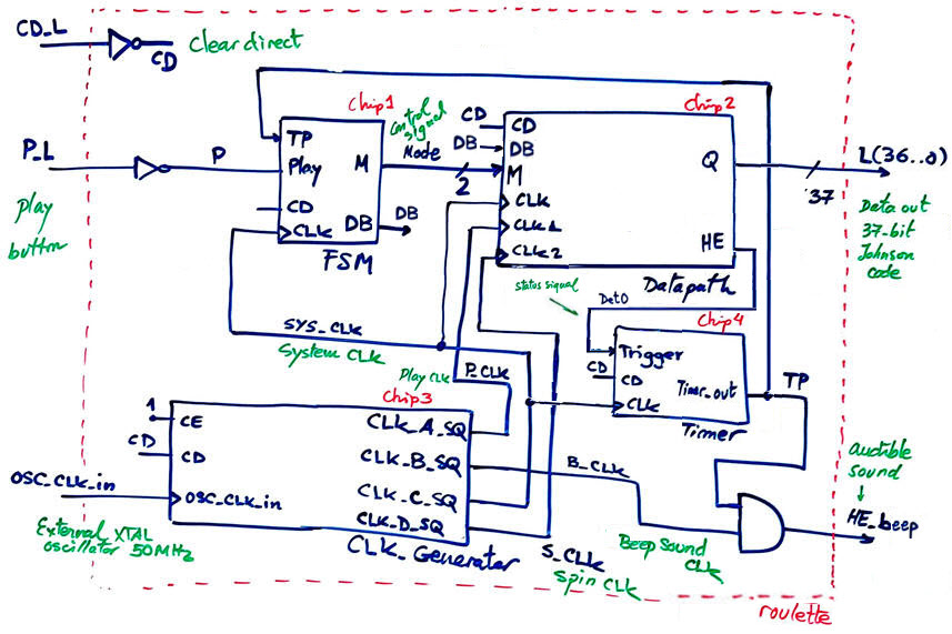
The top architecture for the project is the dedicated processor represented in Fig. 3. The control unit samples the play push button and generates operational modes for the datapath.
Sampling buttons is carried out at the low frequency fSYS_CLK , for instance 200 Hz (the value to use is set as an option) as we did in other applications based on buttons and keys.
In order to generate a random number from 0 to 36, we can imagine the datapath counting (playing) at high frequency fP_CLK, for instance 55.555 kHz (the value to use is set as an option). The FSM will order when to start and stop counting.
To see the wheel spinning while playing we can use another low frequency fS_CLK such 62.2 Hz (the value to use is set as an option).
When the betting result is zero (house edge), the datapath triggers a timer to generate a beep sound for a given timing period TP.
 |
|
Fig. 3. Example dedicated processor showing how several CLK frequencies are used for different functions. |
- Design step #1. FSM
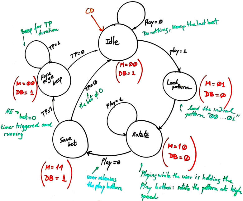
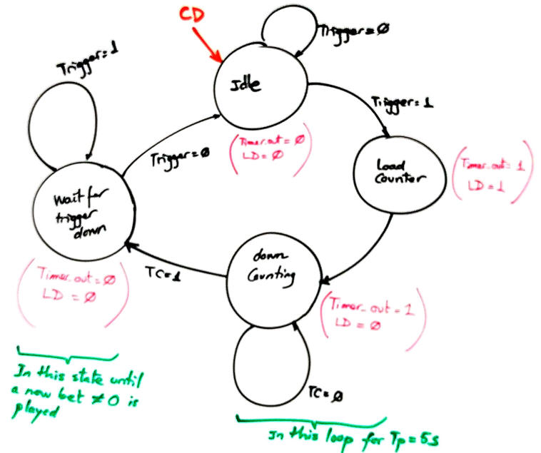
The FSM will run the state diagram below:
 |
|
Fig. 4. FSM state diagram. |
Adapt the FSM architecture to this problem, naming and connecting all signals and inputs and outputs.
Draw the state register memory and deduce the number of D_FF required when encoding the machine using one of the following options:
Option #1: radix-2 (sequential)
Option #2: Gray
Option #3: Johnson
Option #4: one-hot
Draw the CC2 truth table to obtain the circuit's outputs and its equivalent flowchart behavioural interpretation (plan B).
Draw the CC1 truth table to obtain the circuit's state transitions and its equivalent flowchart behavioural interpretation (plan B).
Project location:
C:\CSD\P6\roulette\(files)
Write the FSM VHDL file.
Start a Quartus Prime synthesis project for one of the following programmable target chips:
Option #1: Cyclone IV EP4CE115F29C7
Option #2: MAX II EPM2210F324C3
Option #3: MAX 10 10M50DAF484C7 (*)
(*) Remember that this chip does not generate sdo delay files, thus use another one when gate-level simulations are required.
Inspect and annotate the RTL and technology views. Check the number of D_FF synthesised in this application.
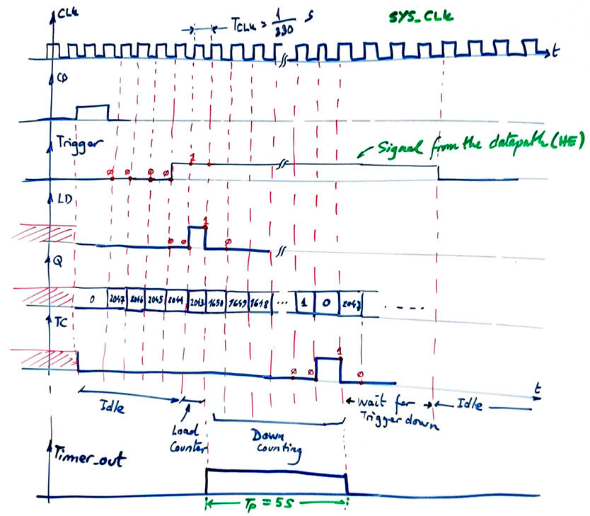
Generate a VHDL testbench fixture schematic. Translate the timing diagram sketch from the specifications into de corresponding stimulus processes.
Run functional simulations to verify your design. Visualise as well the internal states in the wave timing diagram.
Run gate-level simulations to measure the propagation time CLK to output (tCO). Measure the minimum TCLK period or the maximum frequency of operation of the FSM.
- Design step #2. Datapath
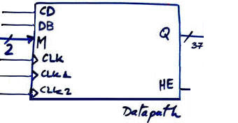
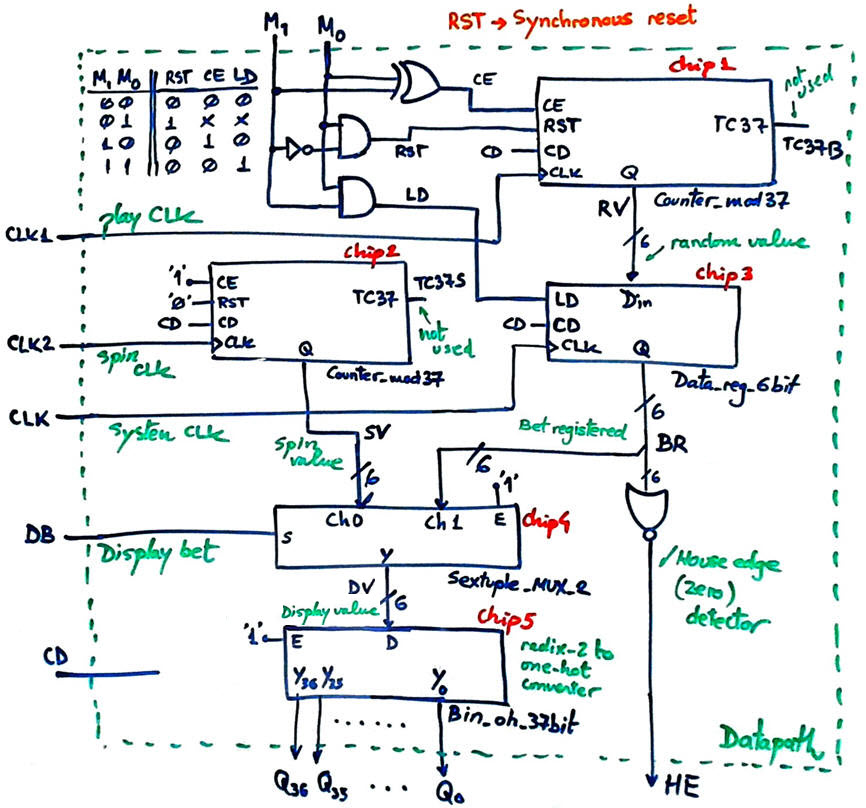
This component provides the operational resources for generating random numbers and driving the LED wheel. It has four modes of operation as shown in its function table. We aim to design it as well using a plan C2 architecture of combinational and sequential components.
 |
|
Fig. 5. Datapath symbol and function table. |
Datapath version #V1. Counting in binary radix-2
The control signal M from the FSM is decoded to control the operation of counters and registers, as shown in Fig. 6.
 |
|
Fig. 6. Option #1 datapath internal architecture. |
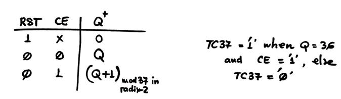
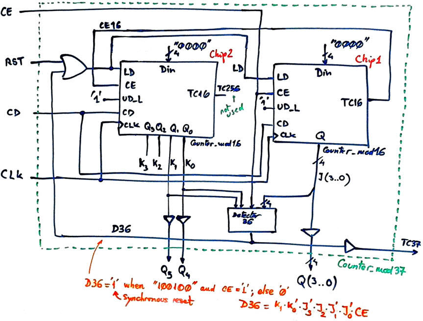
Use the building block Counter_mod16 for implementing the Counter_mod37 used two times as Chip1 and Chip2. Be aware that it contains a priority synchronous reset control signal RST as shown in Fig. 7.
 |
|
Fig. 7. Counter_mod37 function table. |
As indicated in Fig. 8, we can use two components chained to reach modulo 256. And then truncate the count at 36. This signal D36 is ORded with the external synchronous reset RST.
 |
|
Fig. 8. Counter_mod37 based on truncating a radix-2 counter modulo 256. |
Plan and develop the datapath and the FSM. Write the VHDL files and start an EDA project to synthesise the circuit for an FPGA target chip. Inspect the RTL and verify that it looks like your schematic. Check the number of D_FF used in this application, print and comment the schematics.
Project location:
C:\CSD\P7\roulette2\(files)
Datapath version #V2. Counting in BCD
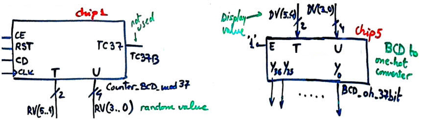
Redraw the same datapath structure in Fig. 5 but replacing binary radix-2 counters Chip1 and Chip2 by Counter_BCD_mod37, as shown in Fig. 9. We will also replace the decoder Chip5 by a BCD_oh_37bit.
 |
|
Fig. 9. Option #2 Counter_BCD_mod37 and one-hot decoder. |
Let us design the Counter_BCD_mod37, a synchronous two digits BCD modulo 37 [00, 01, 02, ..., 09, 10, 11, ..., 36, 00, 01, ...] up counter. We will follow structural VHDL plan C2 using EDA tools and counter chaining and truncation techniques. The building block for counting is our Counter_mod16 and other combinational components and logic. The internal schematic is presented in Fig. 10.
 |
|
Fig. 10. The idea of a BCD counter modulo 37 and the logic behind count truncation. A similar example is studied in P7 highlighted project on an Hour_counter (or Counter_BCD_mod24). Modify it as in Fig. 8 to introduce the RST. |
We an also implement the BCD to one-hot adapter to fit the truth table in Fig. 11.
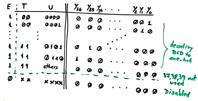 ç ç |
|
Fig. 11. BCD_oh_37bit decoder truth table. |
Plan and develop the datapath and the FSM. Write the VHDL files and start an EDA project to synthesise the circuit for an FPGA target chip. Inspect the RTL and verify that it looks like your schematic. Check the number of D_FF used in this application, print and comment the schematics.
Project location:
C:\CSD\P7\roulette2\(files)
Datapath version #V3. Shift registers and bit rotation
Invent and develop the datapath for this application. It includes shift registers components such Shift reg_4bit connected to expand to 37 LED and also allow bit rotations.
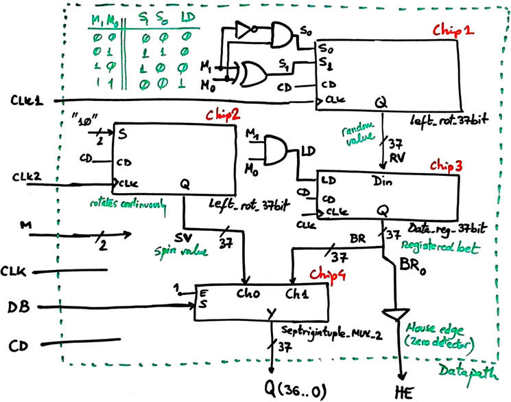 |
|
Fig. 12. Option #3 datapath internal architecture. The correct name of the 37-tuple MUX_2 can be found in this link. |
For example, Fig. 13 shows how a 40-bit shift register can be invented for the specific 37-bit left rotator required for this application.
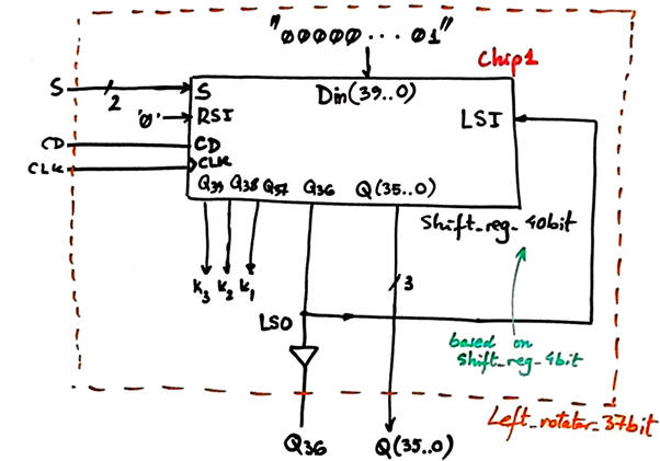 |
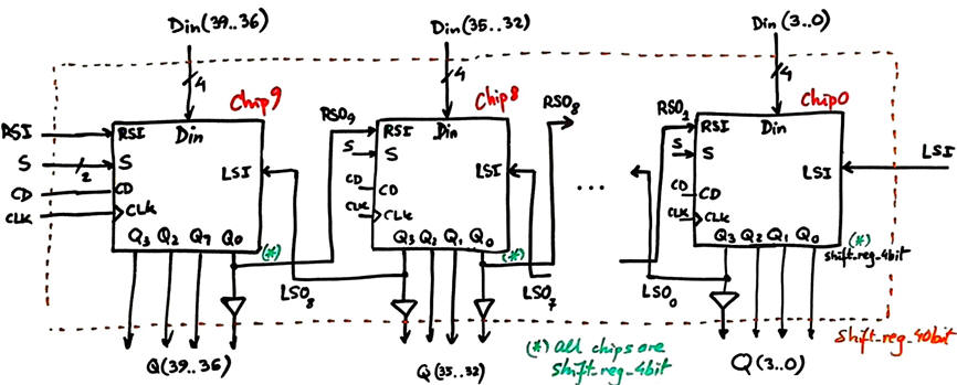 |
|
Fig. 13. The idea of a datapath based on shift-registers and (left) bit rotation. This datapath may be used while betting (keeping pressed the play button). It yet has to be modified for showing as well the wheel of LED spinning at a much lower speed. |
Develop the datapath and the FSM. Write the VHDL files and start an EDA project to synthesise the circuit for an FPGA target chip. Inspect the RTL and verify that it looks like your schematic. Check the number of D_FF used in this application, print and comment the schematics.
Project location:
C:\CSD\P7\roulette\(files)
- Design step #3. CLK_Generator
Design the CLK generator circuit Chip3 in Fig. 3 from a 50 MHz quartz crystal oscillator to obtain all the clocking signals required to drive the application. Deduce the number of D_FF required for this component. Add this Chip3 to the top architecture.
 |
|
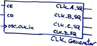
Fig. 14. CLK generator symbol. |
Project location: C:\CSD\P8\roulette\(files)
Your instructor will assign you a set of frequencies:
Option #1: fP_CLK = 55.556 kHz; fB_CLK = 1.2 kHz; fSYS_CLK = 202 Hz; fS_CLK = 26 Hz;
Option #2: fP_CLK = 67.6768 kHz; fB_CLK = 1.6 kHz; fSYS_CLK = 189 Hz; fS_CLK = 21.15 Hz;
Option #3: fP_CLK = 58.897 kHz; fB_CLK = 1.35 kHz; fSYS_CLK = 219 Hz; fS_CLK = 16.5 Hz;
- Design step #4. Timer
(optional, only if you have spare time and the previous design steps work correctly).
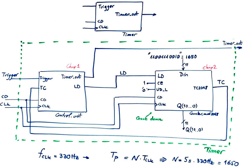
The Timer Chip4 in Fig. 3, is for beeping several seconds at fB_CLK when the house edge HE value 0 is generated. This flag will trigger the timer period. The Fig. 15 is an example of timer that you can adapt to your SYS_CLK option. For example, design a Timer for TP = 5 s from fSYS_CLK = 330 Hz. We use a down-counter that counts N CLK periods when triggered.
   |
|
Fig. 15. Timer symbol and ideas for designing it. |
Synthesise the project verifying the total number of D_FF.
Draw a testbench fixture to check how to complete dedicated processor roulette works.
Design phase #2: Idle indication sequence (optional, only if you have spare time and the design phase #1 works correctly) phase
After a given display timing period tPD (options below) of not touching P_L, the roulette starts to visualise an idle sequence of LED in movement rotating slowly a pattern right and left while generating audible tones, to show that it is still active and waiting for the user to play the next bet. Therefore the circuit keeps the last bet LED lighting only for the timing period.
Option #1: TPD = 3 min. 22 s.
Option #2: TPD = 2 min. 34 s.
Option #3: TPD = 1 min. 56 s.
How to enhance the datapath and the FSM state diagram?
An idea that may be considered and put into practice for generating a moving sequence is subsampling at low frequency, for instance fS_CLK, the current random value.
|
Fig. 15. Datapath enhanced to generate an Idle sequence and audible tones. |
Project location:
C:\CSD\P8\roulette2\(files)
| Home Term 26/27-Q1 Contact Products Electronic devices and companies Software Books Magazines Instruments DEE Library EETAC DEEL |

|
|
| Web activa des de 09/2001, @ F. J. Robert, Web editat amb Microsoft Expression Web 4. El contingut és un complement als materials d'estudi del curs Circuits i Sistemes Digitals disponibles al campus digital Atenea. Llicència:Reconeixement 4.0 Internacional de Creative Commons |