|
|
Bachelor's Degree in Telecommunications Systems and in Network Engineering |
|
Chapter 1 problems |
- D1.17 - |
3-digit BCD adder / subtractor for unsigned numbers |
Design a 3-digit adder-subtractor for unsigned BCD numbers (Add_Subt_BCD_3digit) using algorithms that include only Adder_4bit modules, applying plan C2. We have two version of such basic block from tutorials: (1) RC ripple-carry Adder_4bit, (2) carry-lookahead Adder_4bit.
The same project B3.17 is proposed in Chapter 3 for learning the basics of μC software organisation and basic digital I/O.
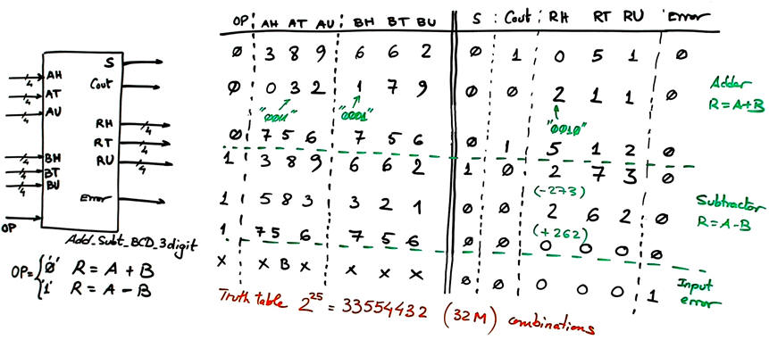
The circuit symbol and truth table is represented in Fig. 1. 3-digit numbers A, B, allows representing one thousand input values as hundreds, tens and units. Results are positive or negative, thus, an additional output S will be required to indicate negative results. When adding is possible to set the Cout signal for results larger than one thousand. We will include the Error signal that detects when the inputs contain illegal codes.
 |
|
Fig. 1. Symbol and some truth table values. |
What is the range of operands and results? You can consider several options for A and B the test vectors:
option #1: Numbers 767, 732, 0, 177, 999, 5
option #2: Numbers 393, 855, 87, 414, 0, 2
option #3: Numbers 938, 879, 98, 0, 17, 166
Experiment with several input vectors and calculate the outputs. Draw the truth table. How long is it?
Draw an example of timing diagram to be used later as stimulus in the testbench when verifying the synthesised circuit. Consider Min_Pulse = 2.13 μs. How long does it take to simulate all the truth table combinations?
2. Planning
Adding in BCD
A project like this one admits multiple solutions.
Option #1: one way to do it is converting input operands into radix-2 is proposed as Annex 1 for two digits.
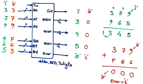
Option #2: Adding in BCD (Adder_BCD_1digit) is possible using radix-2 adders and correcting the result when larger than 9 or when Cout = '1' as presented in Fig. 2 (each radix-2 sum should be adjusted to skip the six unused codes). Fig. 3 shows the truth table of this Chip2 BCD_ corrector. This circuit is also used as the highlighted tutorial in P9, and it was manufactured as an standard classic CMOS chip MC14560 by Motorola (now NXP). This device allows rippling carries to attain any number of digits. We add an error detector, Error = '1' when A or B contain a illegal input code.
 |
|
Fig. 2. Proposed internal design for the circuit Adder_BCD_1digit component. |
You can propose internal circuits for Chip3 and Chip4. For instance, the BCD_Corrector truth table is represented in Fig. 3 and can be easily captured in Minilog and solved using plan A equations on PoS or SoP.
 |
|
Fig. 3. BCD corrector algorithm. Try several numbers to validate the truth table. |
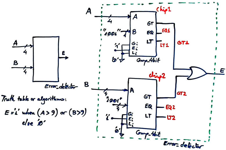
For instance, the Error_detector algorithm and plan C2 implementation is shown in Fig. 4. The component Comp_4bit is listed in digsys products page.
 |
|
Fig. 4. Error_detector algorithm and proposed circuit based on plan C2 using CSD comparators. |
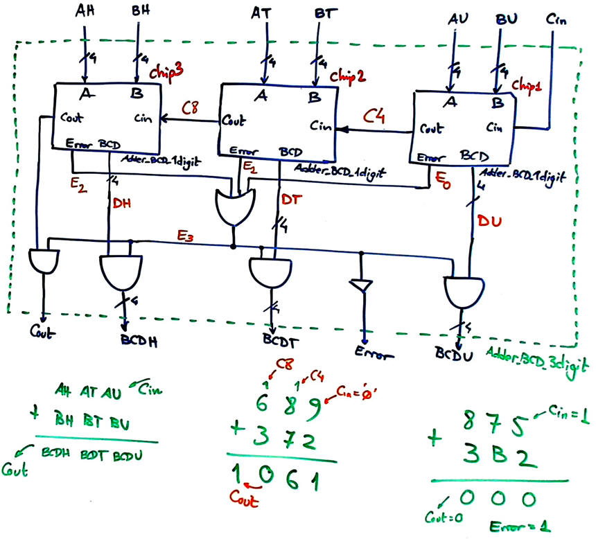
The next Fig. 5 and Fig. 6 show how through rippling carries we can generate an Adder_BCD_3digit.
 |
|
Fig. 5. Proposed top block diagram for the expandable Adder_BCD_3digit. |
 |
|
Fig. 6. Internal architecture for the Adder_BCD_3digit. When inventing such structures you have to try several vectors to validate it before developing and testing it. |
Subtracting in BCD
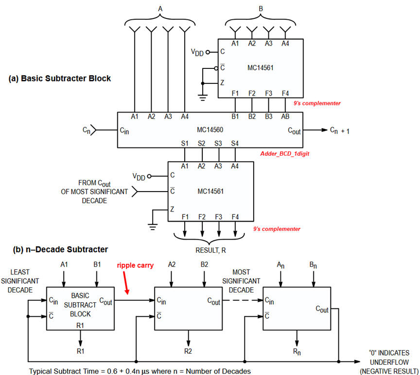
Subtracting directly BCD numbers is possible using the 9's complement (9C), as it is subtracting in radix-2 using the 2's complement (2C) and adder devices (see the highlighted P4). The 9's complement is calculated for each digit subtracting the operand from 9, as shown in D1.2. Alternatively, a true subtractor is proposed in D1.13.
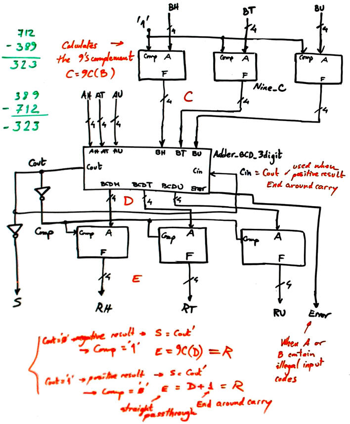
Let us discuss with some examples the subtraction algorithm for unsigned BCD numbers, as shown in Fig. 7. We can adapt the schematic proposed in the datasheet MC14560 using our modules, as shown in Fig. 8.
 |
|
Fig. 7. Example operations and deduced algorithm to subtract in BCD. |
 |
|
Fig. 8. Circuit for building a subtractor for 3-digit BCD numbers. Try some numbers and check that it works. |
Adding and subtracting in BCD
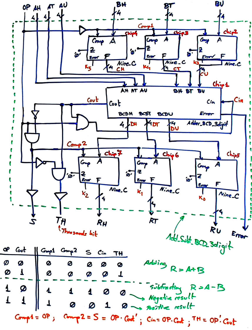
In this problem, we will try to combine both operations in a single circuit as represented by the symbol in Fig. 1. We will use a similar approach when working with integer arithmetic in 2's complement. The input OP will decide how to employ the Nine_C, as straight-through for adding OP = '0', F = A; or as the 9's complementer OP = '1', F = 9C(A). Thus, we can modify lightly the Fig. 8 circuit to generate the control signals as shown in Fig. 9. The thousands TH bit is only used when adding. The sigh S is only used when subtracting and in case of a negative result. Cin is only used when subtracting and with a positive result.
 |
|
Fig. 9. Plan ready for VHDL translation for the Add_Subt_BCD_3digit. |
3. Development
Circuit synthesis. FPGA target chip options:
option #1: MAX II
option #2: MAX 10
option #3: Cyclone IV
4. Test (functional)
Functional simulation.
After having studied P4 lectures and Lab 4.1 tutorials, the project can continue adding the fifth section below on time measurements and characterisation.
5. Test (gate-level)
Additional questions can be added to our report. For instance:
-
Perform a gate-level simulation to measure propagation delays in a given signal transition.
-
Deduce the worst-case propagation delay running the timing analyser tool and calculate the circuit's maximum frequency of operation for the target chip used in the design.
-
In the end, because two alternative circuits are proposed (option 1 and option 2), we can compare which one is faster and which one uses less resources (logic elements).
Annex 1: Design a 2-digit BCD adder using radix-2 arithmetic
For two digits, and with the help of BCD-to-binary and binary-to-BCD code converters, we can operate in BCD using an Adder_8bit, as shown in Fig. 1.
  |
|
Fig. 1. Proposed top block diagram for the Adder_BCD_2digit with a radix-2 adder. The example operation shown is the truth table maximum computable value. Illegal input operands will generate error. |
The 74184/185 datasheet shows the basic components BCD to binary radix-2 modulo 40 converter (DM74184) and also the basic 6-bit binary radix-2 to BCD converter (DM74185). The idea is that the basic DM74185 expandable block can be adapted and solved in a flat single VHDL file using plan B (copying truth tables) Bin_BCD_6bit or plan A (minimising equations) Bin_BCD_6bit. And, in the same way, the DM74184 can be adapted using plan B as shown in the tutorial BCD_bin_mod40 example.
From the same datasheet we learn how to expand converters to a larger number of bits or digits. More ideas can be found in assignments D1.15 and D1.16. In this project a BCD_bin_2digit and a Bin_BCD_8bit chips will be required.
Project location:
C:\CSD\P3\BCD_adder_2digit\(files)
To make the design simpler and easy to debug and also for obtaining partial marks, we usually organise the complete project in several steps. Think how to grow this circuit so that you can complete the full schematic in several steps.
Using Fig. 2 ideas generate the schematic for the component Bin_BCD_8bit ready for VHDL translation.
  |
|
Fig. 2. In the datasheet we find information on how to expand several bin-to-BCD converter (Bin_BCD_6bit) to obtain our Chip3 Bin_BCD_8bit. |
Using Fig. 3 ideas generate the component BCD_bin_2digit ready for VHDL translation.
  |
|
Fig. 3. In the datasheet we find information on how to expand several BCD-to-binary radix-2 converter (BCD_bin_mod40) to obtain our Chip4 and Chip5 BCD_bin_2digit. |
| Home Term 26/27-Q1 Contact Products Electronic devices and companies Software Books Magazines Instruments DEE Library EETAC DEEL |

|
|
| Web activa des de 09/2001, @ F. J. Robert, Web editat amb Microsoft Expression Web 4. El contingut és un complement als materials d'estudi del curs Circuits i Sistemes Digitals disponibles al campus digital Atenea. Llicència:Reconeixement 4.0 Internacional de Creative Commons |