|
|
Bachelor's Degree in Telecommunications Systems and in Network Engineering |
|
|
|
||
|
|
Comp_1bit plan C2: structural hierarchical multiple-file VHDL |
|
|
|
||
Designing a 1-bit expandable comparator using the method of multiplexers (MoM)
1. Specifications
Design a 1-bit expandable comparator Comp_1bit using the hierarchical multiple-file plan C2 based on the MoM and a MUX_2 (GT), a MUX_4 (EQ) and a MUX_8 (LT). Rec.
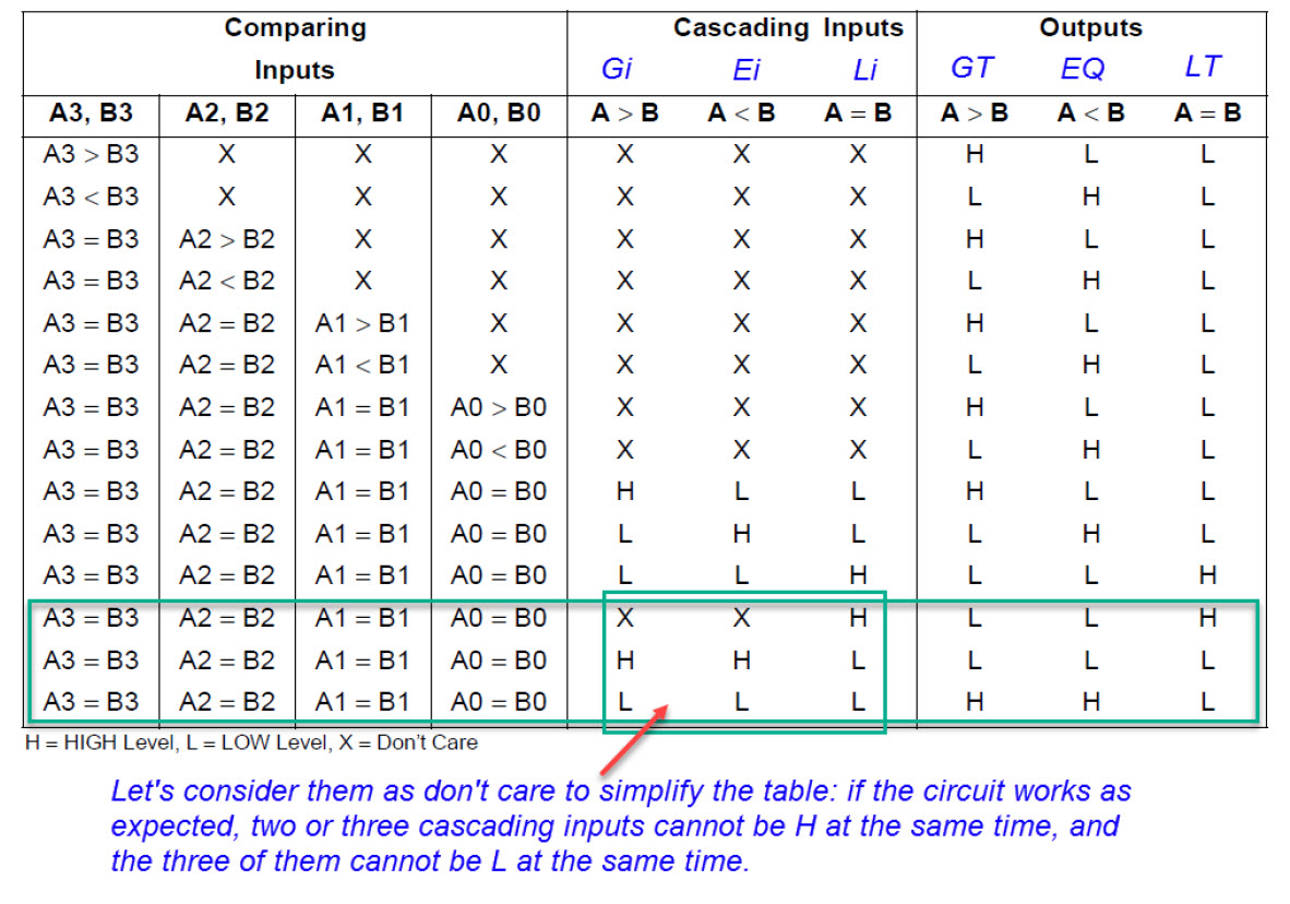
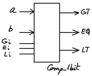
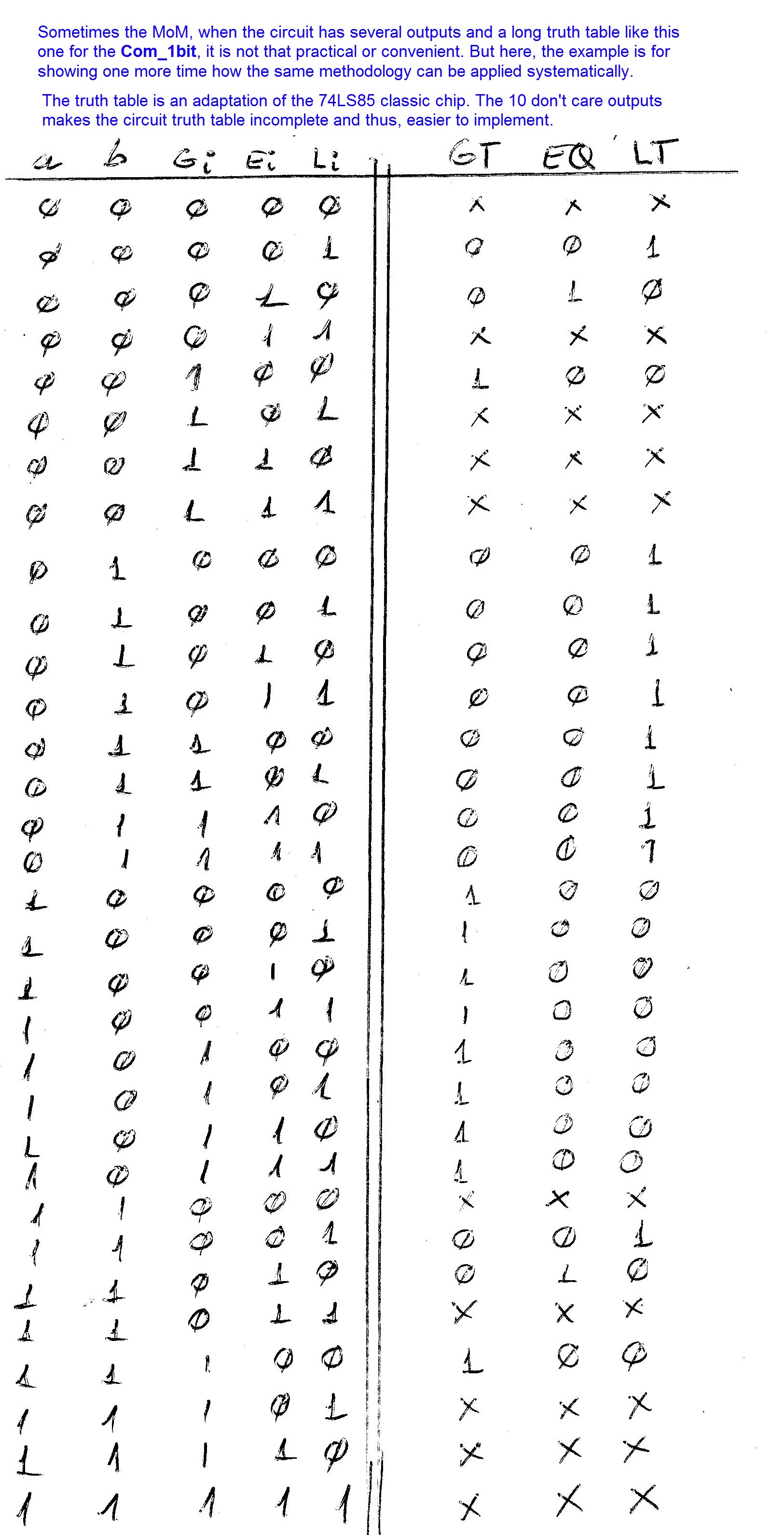
The circuit has the symbol and truth table represented in Fig. 1. The truth table has been adapted from the standard 4-bit commercial comparator chip 74F85, (or 74LS85) the datasheet of which can be used to figure out how to chain comparator components to obtain larger circuits of the same kind. This design is another demonstration on how to apply the method of multiplexers (L3.3) for implementing logic functions.
 |
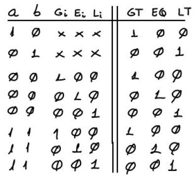 |
Fig. 1. Symbol and truth table of a 1-bit comparator with extra signals for expandability. |
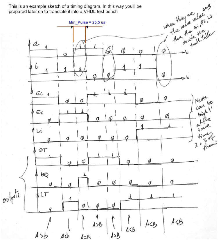
In Fig. 2 there is a simple sketch that represents some values of the truth table in time. The timing diagram will be used in section 4th for testing the circuit using a VHDL testbench. All the 32 combinations can be applied sequentially in time to complete the test.
|
| Fig. 2. Timing diagram where all the inputs are applied sequentially and hence, the output is predicted accordingly to the truth table. |
2. Planning
Plan C2 as an example of using the MoM, a multiple-file hierarchical project.
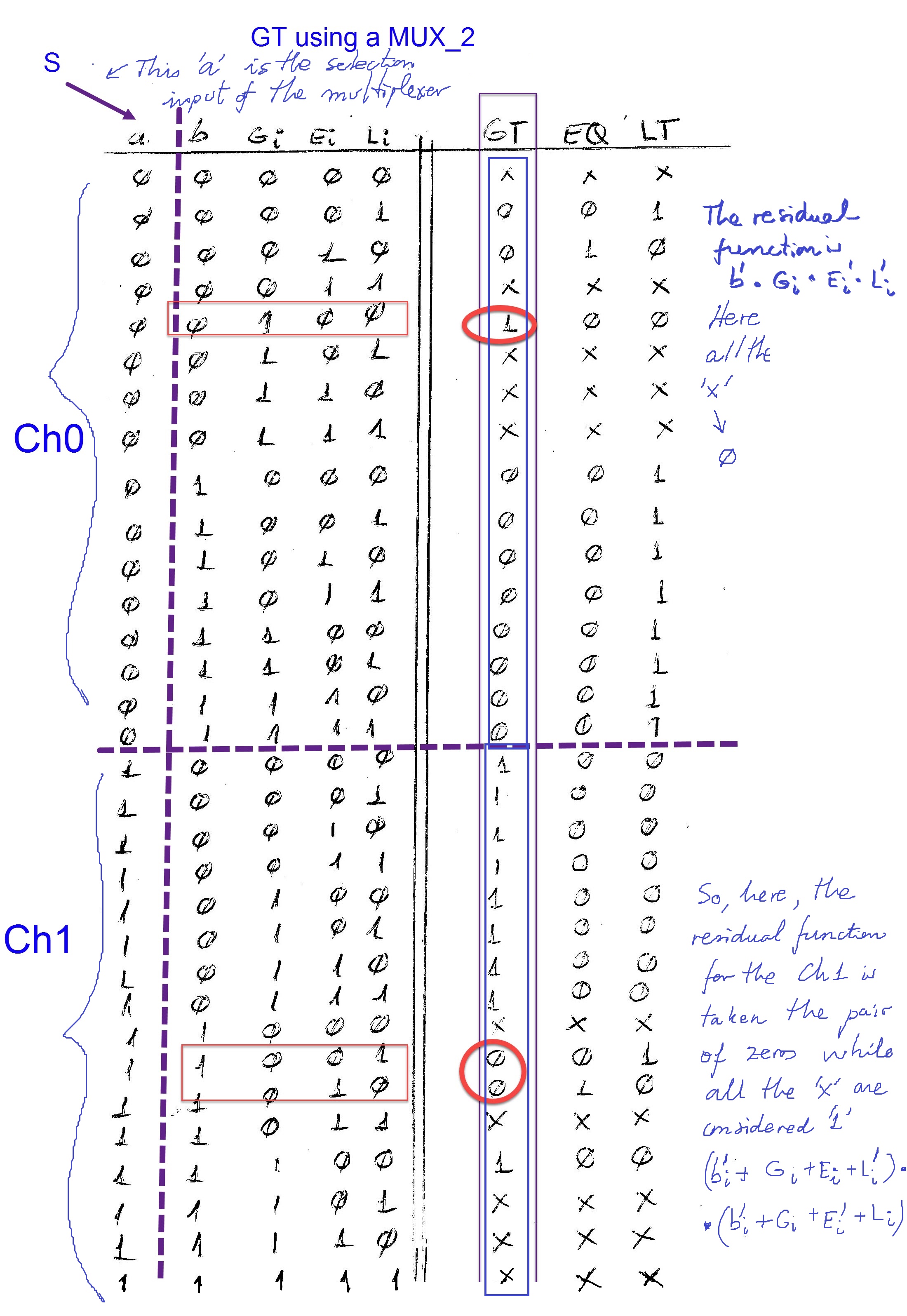
GT = f(a, b, Gi, Ei, Li) using a MUX_2
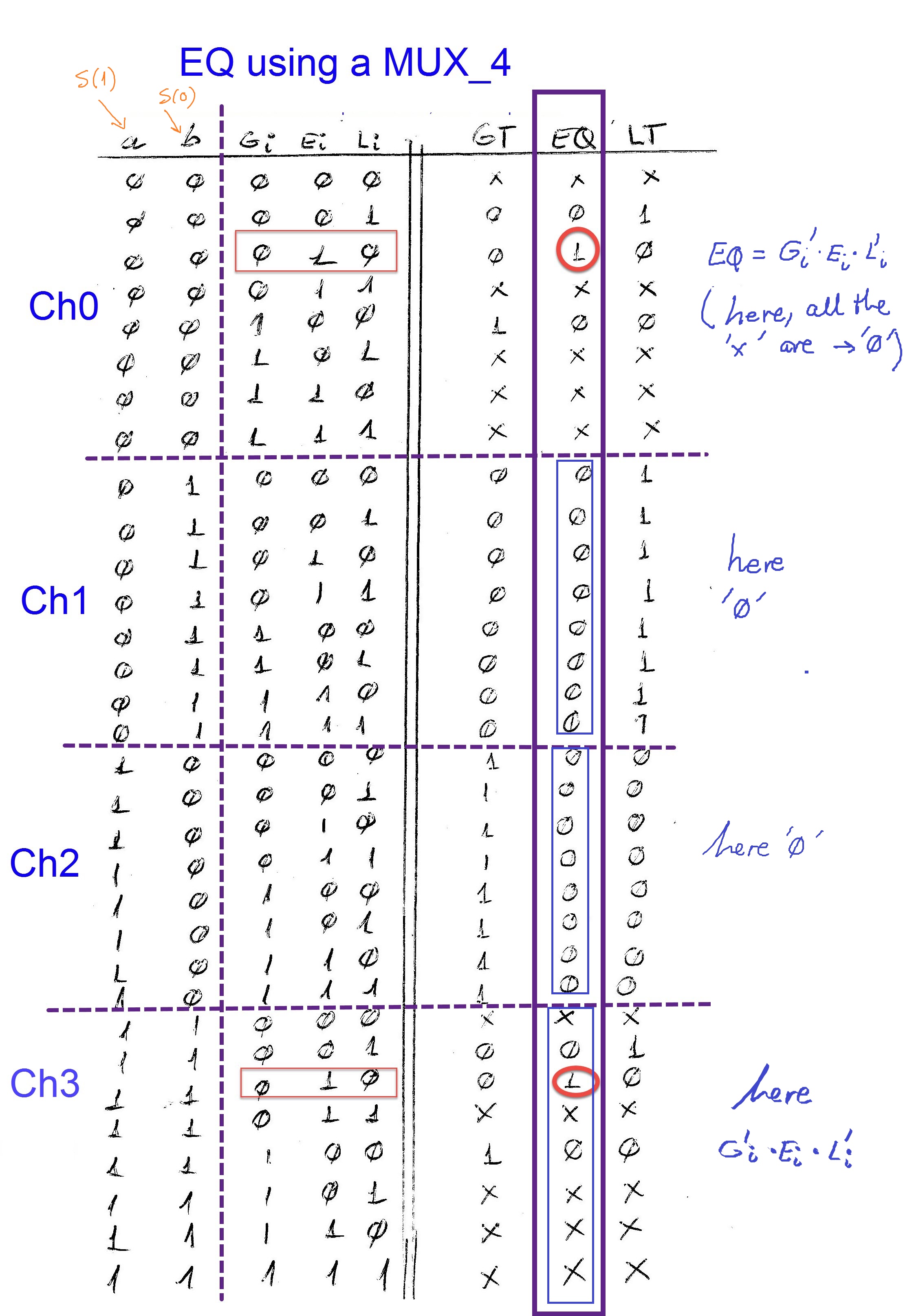
EQ = f(a, b, Gi, Ei, Li) using a MUX_4
LT = f(a, b, Gi, Ei, Li) using a MUX_8
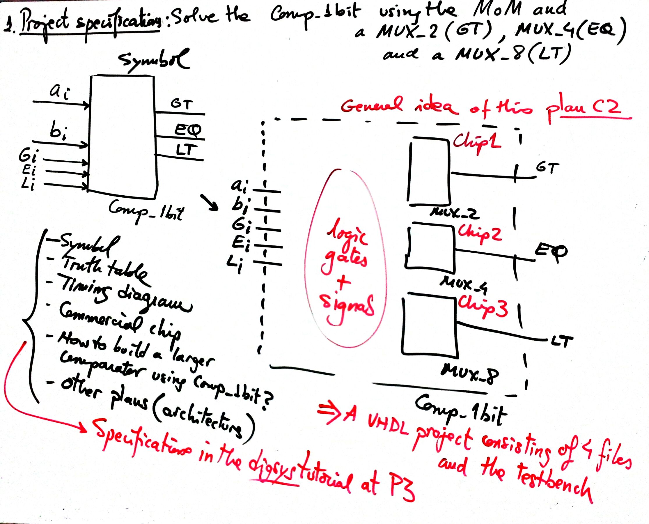 |
Fig. 3. This is the initial idea where we can discuss the approach toward the final circuit implementation. |
Firstly, in this MoM we have to consider the expanded truth table from Fig. 1 and try to subdivide it depending on the number of channels available in the multiplexer in use:
- The organisation of the truth table to infer the GT = f(a, b, Gi, Ei, Li) using a MUX_2
- The organisation of the truth table to infer the EQ = f(a, b, Gi, Ei, Li) using a MUX_4
- The organisation of the truth table to infer the LT = f(a, b, Gi, Ei, Li) using a MUX_8
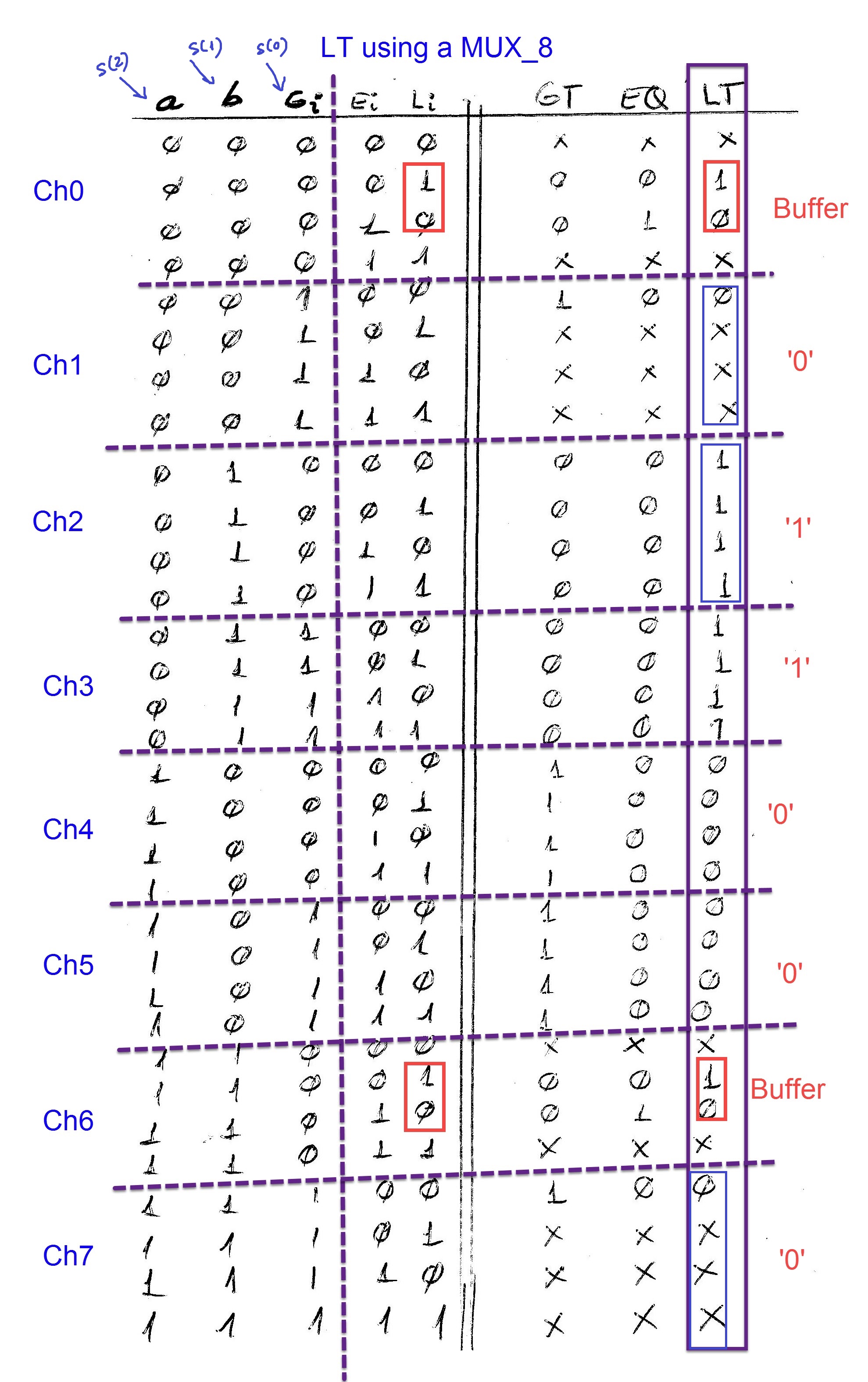
And, secondly, for each output we have to deduce by inspection which is going to be the combinational circuit that will drive each multiplexer channel. And therefore, we draw in paper the final schematic completely annotated with components and signals ready for translation to VHDL as the top entity.
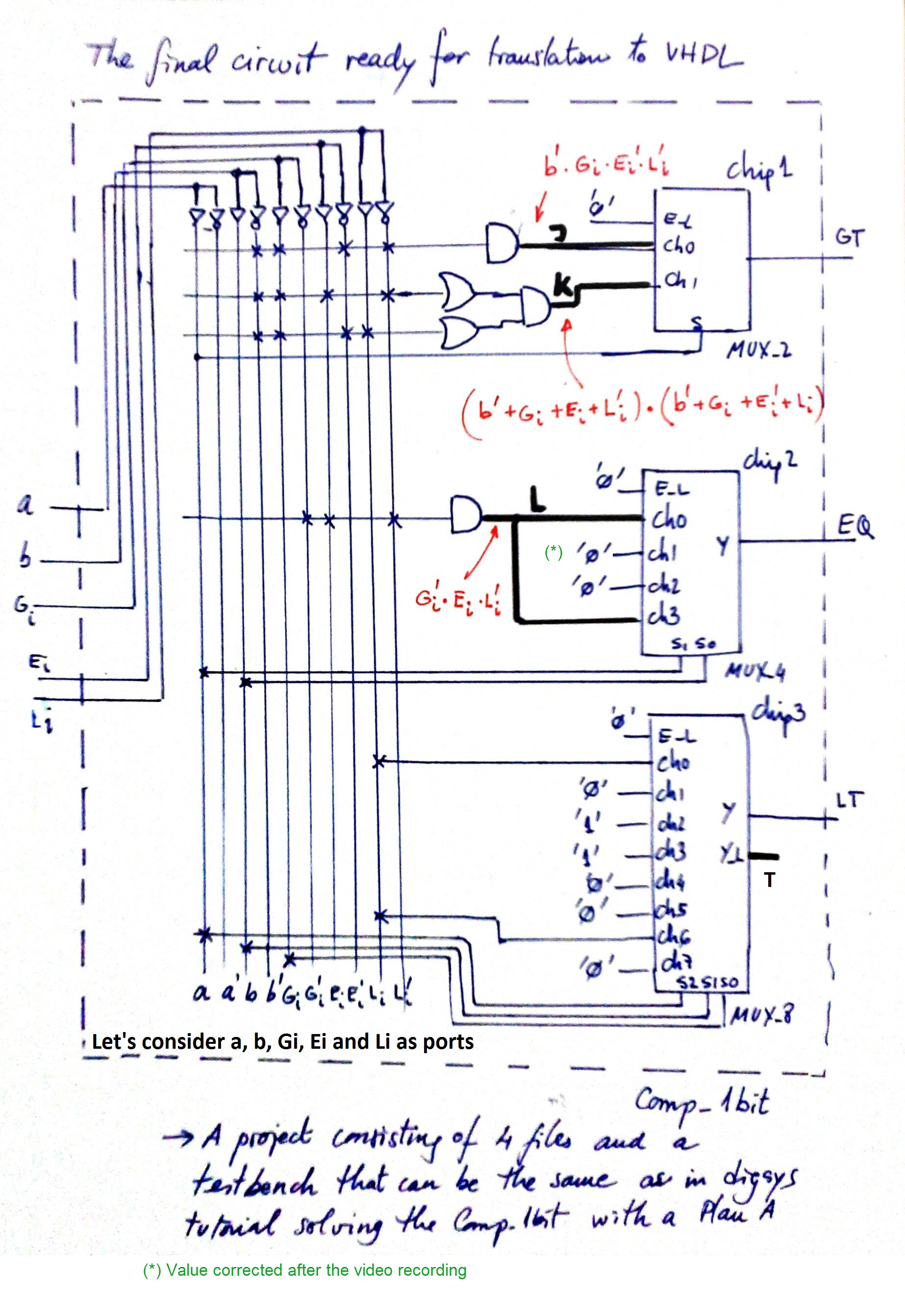
3. Developing the project using EDA tools
Let us synthesise the circuit using an EDA tool. The target chip will be any CPLD or FPGA available in the laboratory from Lattice Semiconductor, AMD or Intel. The project name is Comp_1bit_prj, and the project location:
L:\CSD\P3\Comp_1bit_C2_MoM\(files...)
This is the translation to VHDL of the top Comp_1bit.vhd, and these are the components already used in other designs: MUX_2.vhd, MUX_4.vhd and MUX_8.vhd that has t be included in the same project.
Fig. 4 shows an example of the RTL schematic once the circuit is synthesised for a given target FPGA or CPLD chip.
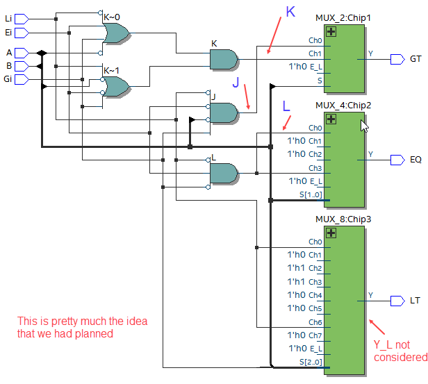 |
| Fig. 4. Example RTL when the project is developed. You can inspect the technology view: How many logic blocks are required? How many Look-up tables? |
4. Testing and validating the design
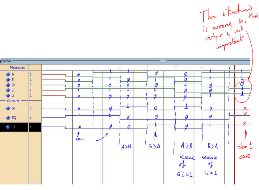
An example test bench Comp_1bit_tb.vhd. Run the VHDL simulation EDA tool to obtain and discuss the timing diagram. Remember that from the testing point of view, even if you have designed the Adder_1bit using several plans, you can use all the time the same testbench.
 |
|
Fig. 5. Example testbench showing results. |
5. Report
Use your sheets of paper, class notes, scanned figures, sketches, VHDL file listings, docx , pptx, or any other resources to write the technical report of this design: Comp_1bit.
Follow this rubric for writing reports.
6. Prototyping
Use training boards and perform laboratory measurements to verify how the circuit works.
| Home Term 26/27-Q1 Contact Products Electronic devices and companies Software Books Magazines Instruments DEE Library EETAC DEEL |

|
|
| Web activa des de 09/2001, @ F. J. Robert, Web editat amb Microsoft Expression Web 4. El contingut és un complement als materials d'estudi del curs Circuits i Sistemes Digitals disponibles al campus digital Atenea. Llicència:Reconeixement 4.0 Internacional de Creative Commons |