|
|
Bachelor's Degree in Telecommunications Systems and in Network Engineering |
|
|
|
||
|
|
2-digit BCD adder and accumulator circuit |
|
|
|
||
| 1. Specifications | Planning | Developing | Test functional | Test gate-level | Report | Prototype |
In this tutorial we show how to adapt to CSD systematic design methodology an example from a book on digital systems: Pons, J., Bardés, D., Mateo, D., Altet, J., "Exercicis resolts de disseny digital", Independently published, 2024.
Using VHDL and EDA tools, design a dedicated processor capable of performing addition and accumulation operations with BCD numbers. The sketch of the circuit from the book (Exercici 3.6) is represented in Fig. 1. This system adds and accumulates sampled BCD values from Din and displays the result Dout as two BCD digits for tens and units. Therefore, the device is capturing and representing BCD numbers and operates in radix-2. Code converters will be used for translating from BCD to radix-2 and the vice versa.
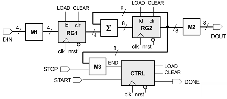 |
Fig. 1. Sketch from the book and proposed symbol for the adder and accumulator dedicated processor. |
The BCD input is a single digit. Non valid BCD input codes will be zeroed (M1 combinational circuit).
An active-low start push-button (START_L) will trigger operations. If start is clicked again while operating the machine resets.
BCD output is two digits. The machine will stop operating when reaching an overflow condition (result > 99) or when an stop click from an active-low push-button STOP_L is detected (M3 circuit). An output pulse DONE indicates this end of operation condition.
In this initial version will consider 1 Hz CLK to be able to input numbers manually using four switches from the prototyping board. The system will be tested in a DE10-Lite board that includes a 50 MHz quartz crystal oscillator. The board's input and outputs resources such push-buttons, switches and 7-segment displays will also be used. Therefore, we can imagine the entity in Fig. 2.
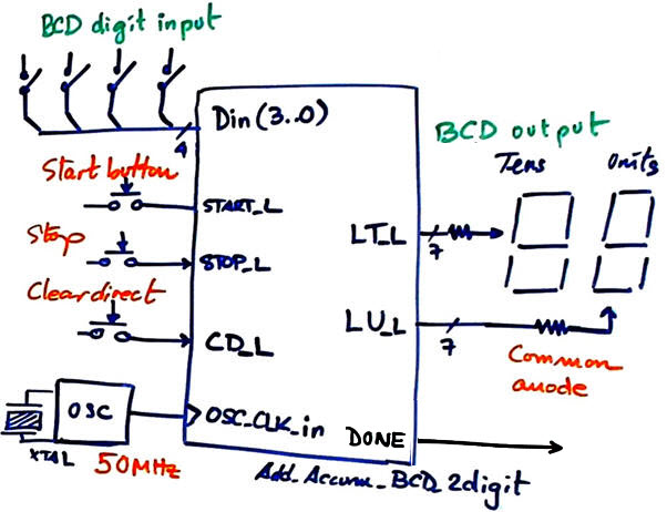 |
Fig. 2. Entity Add_Accum_BCD_2digit. |
To see how the circuit may operate, we better sketch an approximate timing diagram considering some input stimulus and representing expected output values, as shown in Fig. 3. Capturing the current Din value and adding it to the previous accumulated registered value will not be solved at the same CLK edge, thus, at least a CLK cycle delay will be expected.
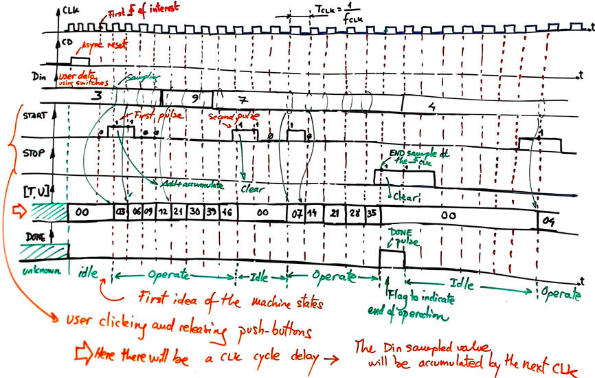 |
Fig. 3. Timing diagram sketch approximation. |
Additional optional steps:
-
In a second step you can add a Debouncing_filter for START and STOP push-buttons to generate clean digital pulses. This feature will require the implementation of a convenient sampling frequency from the CLK_Generator, for instance 100 Hz.
-
Third step we can study how to modify the dedicated processor to add and accumulate at the highest frequency while sensing the push-buttons at 100 Hz.
| Specifications | 2. Planning | Developing | Test functional | Test gate-level | Report | Prototype |
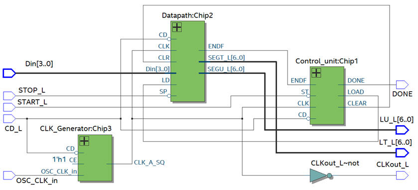
From the initial sketch in Fig. 1, we can infer and draw the system as the dedicated processor (L8.1) represented in Fig. 3.
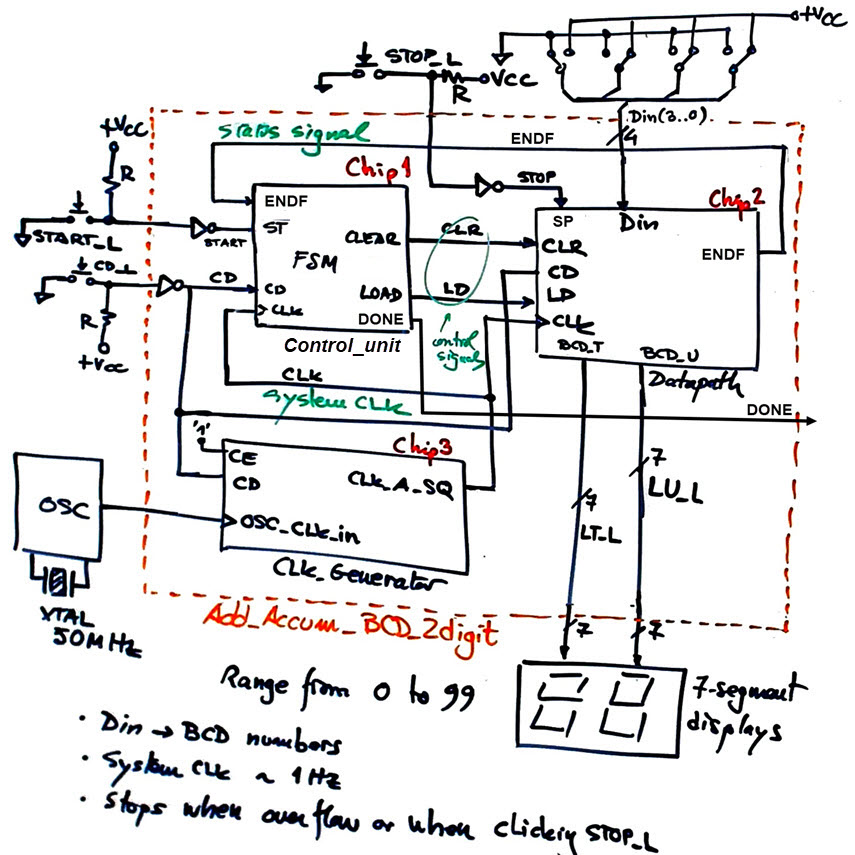 |
Fig. 4. Proposed dedicated processor. |
The datapath will include memory and operational resources and will generate the status signal END for the FSM control unit. We will implement the 4-bit and the 7-bit data registers with synchronous clear CLR signals using plan C2 and our Data_reg_4bit standard circuit. Fig. 5 indicates as well where to find standard components to copy and adapt for this application. For instance, the product Bin_BCD_9bit is available, thus we can use it as a 7-bit binary radix-2 to BCD converter to drive the HEX_7seg_decoder.
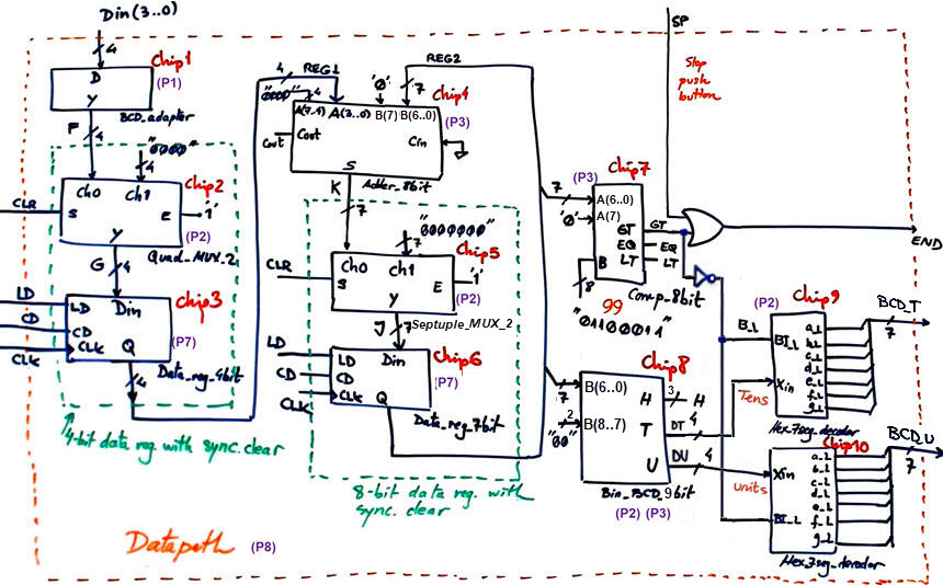 |
Fig. 5. Planning the data-path using components from our library. |
When GT = '1', the REG2 value is larger than '99' and it does not fit correctly in two BCD outputs, thus, this illegal result may be blanked on the 7-segment displays driving BI_L = GT'.
In this initial design step, let us implement a CLK generator (L8.2) with a single 1 Hz square output. Up to 26 D_FF are required for this component drawn in Fig. 7.
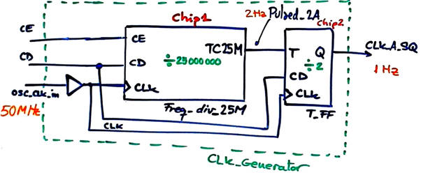 |
Fig. 6. CLK_generator to internal architecture. |
In order to deduce a state diagram for the FSM control unit we have to add several auxiliary states to handle push-button pulses and determine whether they are pressed or released. In this first step we will imagine that such pulses are clean and remain active while the user is clicking as shown in the timing diagram in Fig. 3.
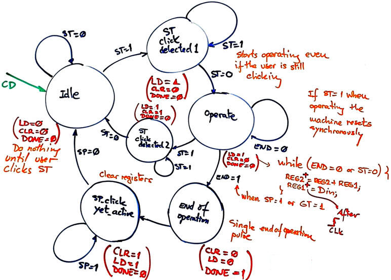 |
Fig. 7. Proposed state diagram to control input push buttons activity and the datapath. |
Infer the number of D_FF that the complete application requires when coding FSM states in Gray or in one-hot.
An option for a more systematic design is to let the control unit interface the STOP push-button in the same way it does with START. In this case, the data-path status signal flag ENDF will be simply the comparator overflow output GT.
Project location:
C:\CSD\P8\Add_Accum\(files)
| Specifications | Planning | 3. Developing | Test functional | Test gate-level | Report | Prototype |
Before starting a Quartus Prime project we translate into VHDL the architecture in Fig. 2 Add_accum_BCD_2digit.vhd and its three main components: CLK_Generator.vhd, Datapath.vhd and Control_unti.vhd and also add to the project the remaining components. This is the full zipped file: Add_accum_BCD_2digit.zip
Picking up the FPGA MAX10 10M50DAF484C7G available in DE10-Lite board, we synthesise the RTL circuit copied in Fig. 7.
 |
| Fig. 8. RTL view. |
The FSM state diagram captured by Quartus Prime is represented in Fig. 9.
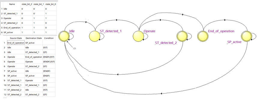 |
Fig. 9. RTL circuit. We can check that this application requires 40 D_FF when encoding states in Gray. |
This design implementation requires up to 124 logic elements.
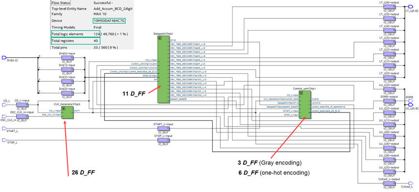 |
Fig. 10. Technology view of this synchronous design. |
| Specifications | Planning | Developing | 4. Test functional | Test gate-level | Report | Prototype |
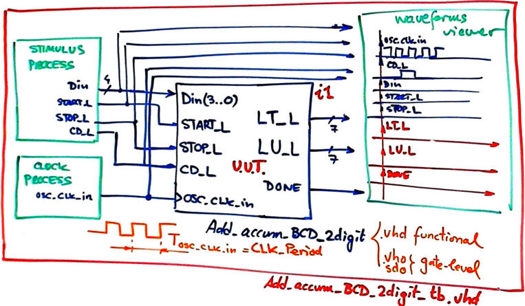
Complete the template test bench file and run the ModelSim EDA tool to detect and correct errors in a functional simulation.
 |
|
Fig. 11. Testbench fixture. |
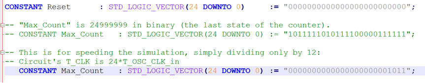
Hint: to speed up simulation, we will imagine for the CLK_Generator a Freq_div_25 instead of the real one Freq_div_25M. We can also imagine CLK_Period = 1 ms. Example Add_Accum_BCD_2digit_tb.vhd.
 |
|
Fig. 12. Adjusting the frequency division a a low value. for speeding simulations. |
Functional simulation results analysing internal signals of interest.
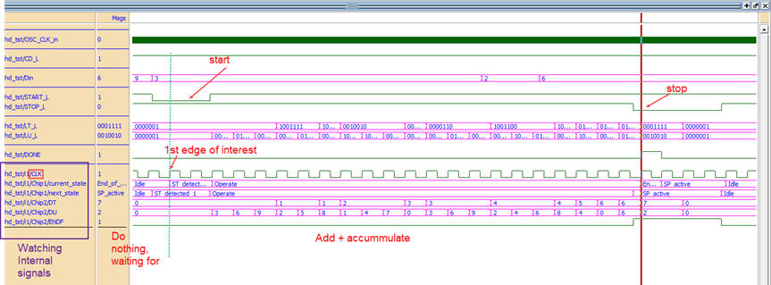 |
Fig. 13. Example of printing functional simulation results. The key idea for correcting errors is monitoring how the states are changing accordingly to the state diagram. |
| Specifications | Planning | Developing | Test functional | 5. Test gate-level | Report | Prototype |
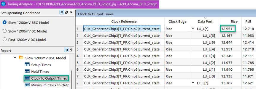
Using the timing analyser tool, let us measure the worst case propagation delay from CLK to output, thus deducing the maximum frequency of operation (76 MHz) if the target chips is the MAX10 FPGA.
 |
|
Fig 14. Timing analyser to measure the maximum speed of operation. |
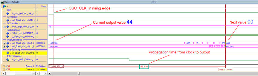
Using a gate-level simulation of the real technology view circuit we can zoom a given CLK transition to observe and measure propagation delays. Consider a Cyclone IV target chip (MAX10 does not generate standard delay files). Fig 15 shows the propagation time from the OSC_CLK_in rise edge to BCD outputs.
 |
|
Fig 15. Gate-level simulations of a given CLK to output transition. |
| Specifications | Planning | Developing | Test functional | Test gate-level | 6. Report | Prototype |
Follow this rubric for writing reports.
| Specifications | Planning | Developing | Test functional | Test gate-level | Report | 7. Prototype |
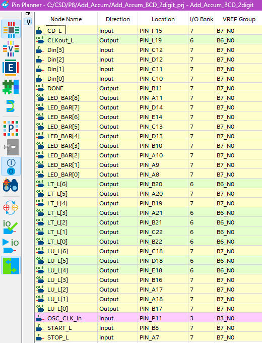
As stated in the specifications, we can use the DE10-Lite board to build the system, assigning inputs, outputs and CLK.
Assignment files Add_Accum_BCD_2digit.qsf and Add_Accum_BCD_2digit_prj.csv.
 |
|
Fig 16. Selecting inputs and outputs for the experiment. |
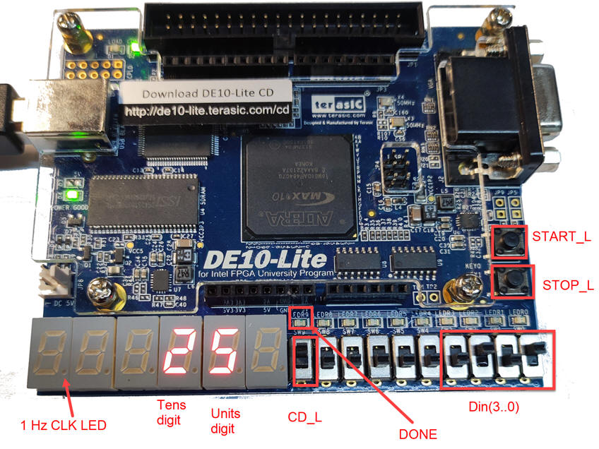
Final picture of the prototype working.
 |
|
Fig 16.Prototype running. |
| Home Term 26/27-Q1 Contact Products Electronic devices and companies Software Books Magazines Instruments DEE Library EETAC DEEL |

|
|
| Web activa des de 09/2001, @ F. J. Robert, Web editat amb Microsoft Expression Web 4. El contingut és un complement als materials d'estudi del curs Circuits i Sistemes Digitals disponibles al campus digital Atenea. Llicència:Reconeixement 4.0 Internacional de Creative Commons |