|
|
Bachelor's Degree in Telecommunications Systems and in Network Engineering |
|
|
Laboratory |
Lab 5: Analysis of circuits based on flip-flops: method I, method II, method III prototype [P5] Method I: pen & paper analysis |
[24/10] |
|
Individual post lab assignment PLA5 to be discussed next Lab6. Study and execute in your computer this lab tutorial before attempting to solve the post lab assignment. |
2.3.7. Analysis of asynchronous and synchronous circuits based on flip-flops and logic
2.3.7.1. Method I: Handwritten pen-and-paper analysis and discussion.
1. Analysis specifications
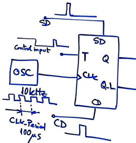
Method I: Analyse the circuit in Fig 1 drawing a timing diagram sketch to see how each flip-flop evolves in time. Determine what kind of output codes are generated after each CLK cycle. What is the function of this circuit? Measure propagation delays CLK to output (tCO) and deduce the maximum CLK frequency fMAX that can be applyed to the circuit.
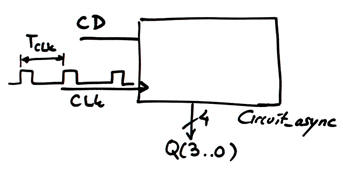 |
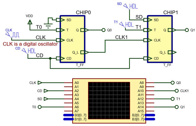
Fig. 1. Symbol and schematic of the asynchronous circuit to be analysed. CLK is a rectangular wave of TCLK period. Clear direct (CD) is a single pulse applied any time the user wants to initialise the circuit. |
 |
|
2. Planning
Step-by-step strategy to gain some practice:
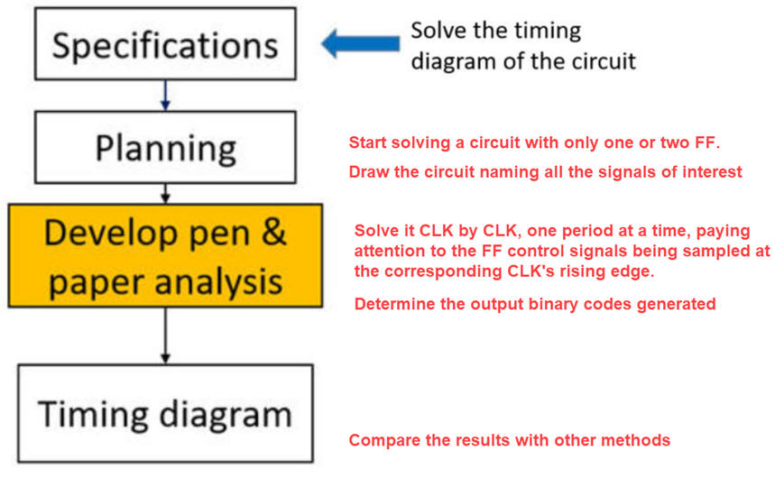 |
Fig. 2. Planning ideas for this handwritten analysis method. |
Step #1: It is better to start solving a very simple circuit, such as a single T_FF driven by a periodic CLK signal and a CD pulse, as it is proposed in its tutorial T_FF. Imagine as well that T is not always '1', but a switching waveform.
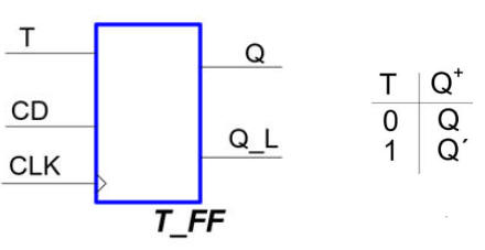 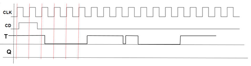 |
Fig. 3. Drive only one FF and apply its function table. |
Step #2: Now, because the circuit is asynchronous (several CLK signals), it is better to imagine what happens when two flip-flops are connected together with different CLK signals. Solve another circuit consisting of two T_FF. What signals are sampled and when?
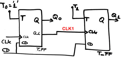 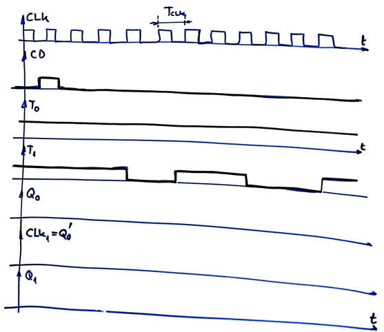 |
Fig. 4. Solve a circuit with two CLK signals. |
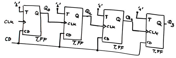
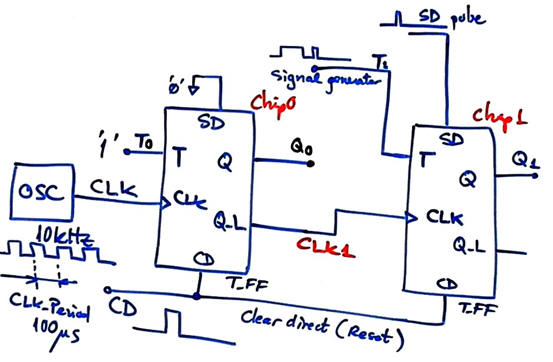
Step #3: Now, it is time to solve the full circuit in Fig. 1. Redraw it and name all the signals of interest, specially CLKs and control inputs.
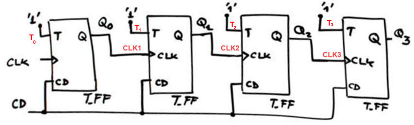 |
Fig. 5. Name all the signals of interest. |
Pictures, notes, scanned materials, theory, etc. can be stored in this project location:
C:\CSD\P5\Circuit_async\paper\(files)
3. Development
Paper work development will follow the step by step strategy organised in the plan.
Step #1: We can drive T with a given wave and solve the output applying the function table. You can do similar exercises with the other D_FF and JK_FF.
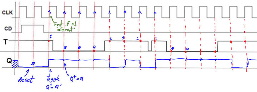 |
Fig. 6. Waveforms. |
Step #2: Identify the number of CLK signals in the circuit. The control inputs sampled values on CLK rising edges will determine the circuit behaviour one CLK period TCLK at a time. TCLK is the circuit's time resolution. Thus, what signals are sampled and when?
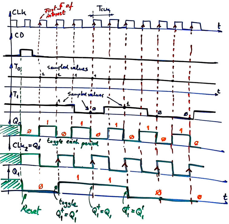 |
Fig. 7. Waveforms indicating the CLK signal rising edges of interest and also the values sampled using dots. |
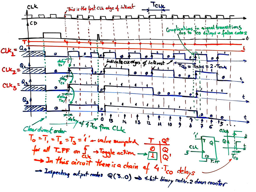
Step #3: With the previous training we can try to analyse the full circuit in Fig. 1 containing four CLK signals. It is asynchronous because rising edges are not going to happen exactly at the same time, thus complicating the analysis.
Be sure to identify what T (or D, JK, RS) input values are sampled at the corresponding CLK's rising edge. To do it, consider the small tCO (in the range of ns) associated to each output transition. Discuss what is happening after each CLK's active edge.
In this circuit, T inputs are always sampled to be '1', as shown in Fig. 3, and the small tCO is not going to be important.
 |
|
Fig. 8. Example of timing diagram and analysis discussion. The complication of this circuit is related to the several CLK signals CLK, CLK1, CLK2, CLK3 delayed each other TCO, and thus false output codes are generated at signal transitions. |
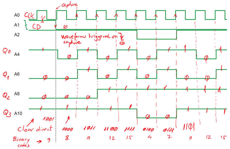
Once the timing diagram is completed, determine the number of states and what is the binary output vector for each state.
The circuit is generating 16 different states: 15 --> 14 --> 13--> .... --> 1 --> 0 ---> 15 --> ... It is a down counting sequence in binary radix-2. Therefore, this is 4-bit down counter running in continuous mode.
4. Test
Compare results with other analysis methods.
5. Reporting
Let us keep each method as a different project. Four sections: 1 + 2 + 3 + 4 for method I. At least four sheets of paper. Follow this rubric for writing reports. Another four sections 1 + 2 + 3 + 4 for the method used to test solutions.
|
Laboratory |
Lab 5: Analysis of circuits based on flip-flops: method I, method II, method III prototype [P5] Method II: Proteus simulation analysis |
[10/4] |
2.3.7.2. Method II: Using Proteus
1. Analysis specifications
Method II: Capture the circuit in Fig 1 in Proteus and run simulations to deduce the timing diagram. Use the logic analyser instrument to represent both inputs and outputs in function of time.
|
|
Fig. 1. Symbol and schematic of the asynchronous circuit to be analysed. CLK is a rectangular wave of TCLK period. Clear direct (CD) is a single pulse any time the user like to initialise the circuit. |
|
|
|
Examples of Proteus latch and flip-flop simulations and technology implementation:
(1) The basic idea of an RS_latch cell (symbol, function table, timing diagram). Run in Proteus and in VHDL the RS_latch.pdsprj example to comprehend how a 1-bit memory cell works.
(2) The basic idea of an RS_FF (symbol, function table, timing diagram). Run in Proteus the RS_FF.pdsprj example to grasp differences with respect a latch. What is the meaning of sampling the value of the cell's control inputs R and S? What is the sampling frequency? How the CLK's rising edge detector works? How the RS_FF internal latch cell is enabled only in the CLK's rising edge?
(3) Circuits including FF to adapt to other projects: CMOS, LS-TTL.
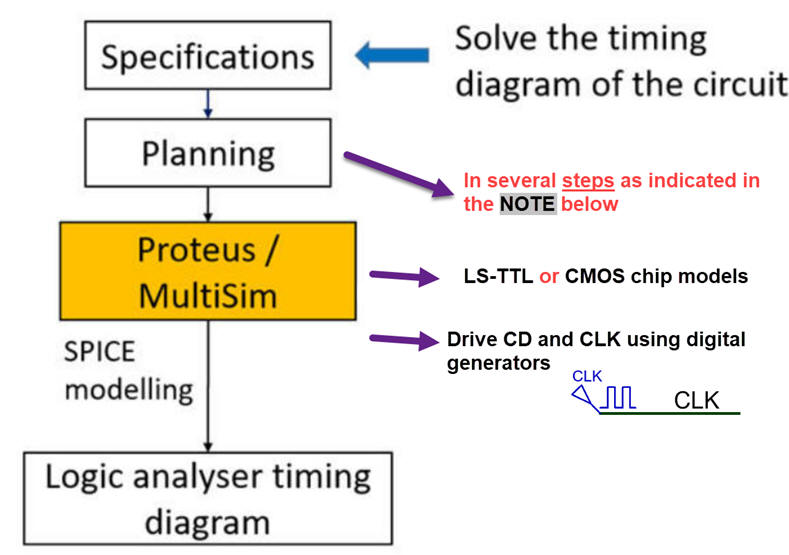
2. Planning
Capture the circuit in Proteus using components modeled on the same logic family and technology in several steps to be able to learn how the FF work and the new instrumentation such digital generators and logic analysers.
 |
|
Fig. 2. Planning method II. |
To complete the plan follow the steps indicated in this note:
|
NOTE
on planning method II on
virtual lab Proteus. Solving
the
LAB5
using Proteus
successfully does not mean simply running the example file
Circuit_async.pdsprj. It means that you
draw and analyse in several steps how does the circuit work
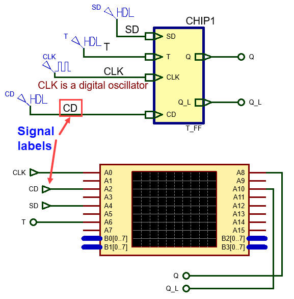
learning at the same time all the concepts involved: Step #1. Only one FF using one of the given seed files to copy and adapt. Use this circuit to learn about CD and SD pulses, oscillators and EasyHDL scripting language for generating input signals.
Let us make it simple and use only simulation models for components from two common libraries: option #1: LS-TTL, find a similar circuit to copy and adapt and name it Circuit_Async_step1.pdsprj option #2: CMOS classic 4000 series, find a similar circuit to copy and adapt and name it Circuit_Async_step1.pdsprj Connect the CLK, CD (and SD if required) stimulus signals using generators or EasyHDL scripting language. Run and observe the waveforms and check that they are what you expect when you solved this single FF in paper method I. For instance, in the T_FF specifications you have a Proteus project with a single FF. Step #2. Draw another circuit with two FF (or two CLK), for example, the same circuit in Fig. 4.
Capture and run again, comparing the new waveforms with your solution in paper method I. Name it name it Circuit_Async_step2.pdsprj Step #3. Complete the LAB5 circuit Circuit_Async.pdsprj in Fig. 1 and check that you get the same results as in method I or method III. Name it Circuit_Async.pdsprj Doing this stepped project you will be able to learn the new logic analyser tool, buses, wires, labels, terminals, power rails, CLK, CD and SD signals, scripting generators in Easy HDL, classic chips, and how memory cells work in time. If necessary do a similar preliminary work with other FF types. This is engineering. The idea is to gain experience and feel comfortable using lab tools before applying them in new unknown circuits. It is the same procedure when you do these experiments for real using lab boards, components and instruments. And the basic experience is gained always from tutorial circuits, reference materials and discussing with team mates. Finally you apply your experience and knowledge analysing new circuits, and the way to be sure that they work or that your solutions are correct is by comparison solving them by other methods. Additional step #4. Try to measure propagation delays from CLK to output (tCO) using the logic analyser knots set in ns resolution. Hint: When picking parts from the library to build your new circuit, do this initialisation from Proteus top menu: --> Tool --> Global Annotator--> Total. This is an example of clean waveforms generated using the Proteus logic analyser in a given circuit. The waveforms are printed and commented (white background as usual to save printer ink, remove the grid and draw vertical lines of interest):
|
Project location:
C:\CSD\P5\Circuit_async\Proteus\(files).
3. Development
Step #1: This is a first circuit containing only one T_FF. CMOS technology: Circuit_Async_step1.pdsprj as in Fig. 3. The same circuit using LS-TTL: Circuit_Async_step1.pdsprj. As we do in VHDL, it is a good idea to reference all time constants to CLK_Period multiples.
 |
|
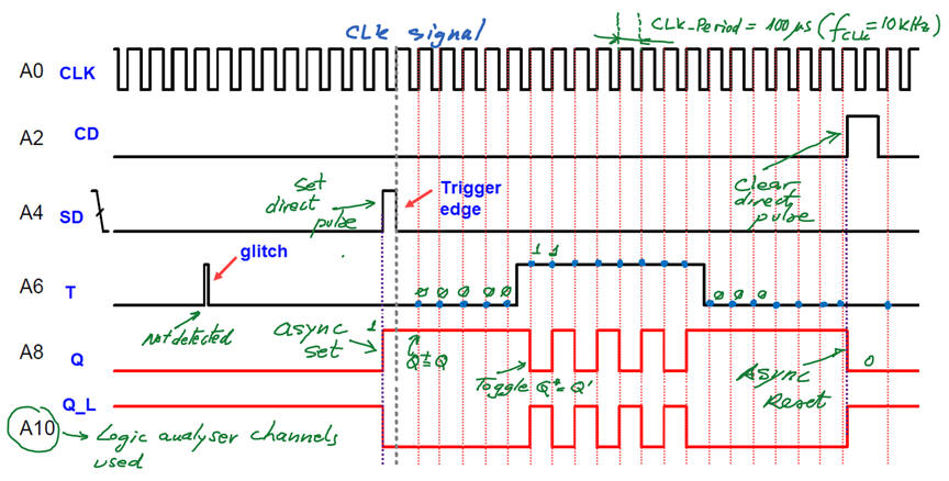
Fig. 6. Only one T_FF driven with CLK, CD, SD and T signals. |
The logic analyser results printing in Fig. 7 shows how the circuit works.
 |
|
Fig. 7. Example waveforms from the circuit with only one T_FF. |
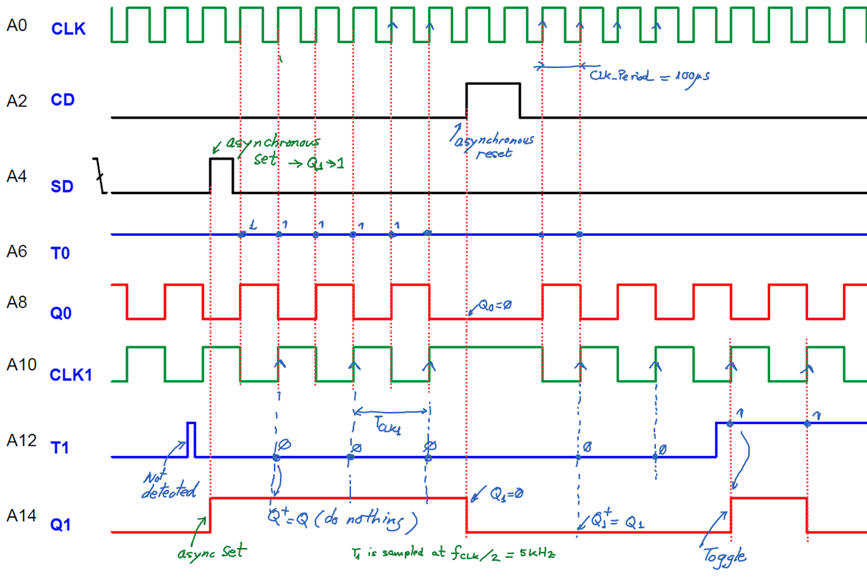
Step #2: Now, we can handle a more complex circuit based on two FF as proposed in Fig. 4. This is the second circuit: Circuit_Async_step2.pdsprj in CMOS technology and Circuit_Async_step2.pdsprj in LS-TTL technology.
 |
|
Fig. 8. Example of circuit with two T_FF driven with CLK, CD, SD and T signals. |
The logic analyser results printing in Fig. 9 shows how the circuit works. Chip1 works only when there is a CLK1 rising edge available.
 |
|
Fig. 9. Example waveforms from the circuit with two FF. See how T signals are sampled with different frequencies. |
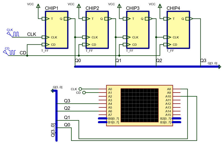
Step #3: Example adaptation Circuit_async.pdsprj for CMOS technology. Example adaptation Circuit_async.pdsprj for LS-TTL technology.
 |
|
Fig. 10. Circuit captured in Proteus. |
Run simulations using the logic analyser instrument and print and discuss results. You will work interactively with instrument windows as in Fig. 11 while working on your analysis.
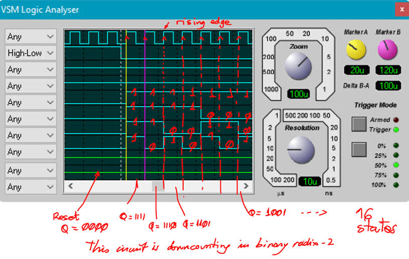 |
Fig. 11. Example of circuit captured in Proteus with logic analyser results. Not recommended per printed report because of the black background and colour visibility. Use in your reports the indications in the note below in Fig. 12. |
The circuit is generating 16 different states: 15 --> 14 --> 13 --> .... --> 1 --> 0 ---> 15 --> ... It is a down counting sequence in binary radix-2. Therefore, this is 4-bit down counter running in continuous mode.
NOTE: When you have completed your analysis, you have to print the instrument windows in white background, removing the grid and unused channels, and above all, adding your handwritten comments as shown in Fig. 12.
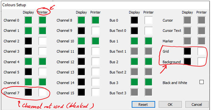 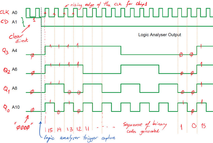 |
Fig. 12. Printed version of the logic analyser instrument window for your project documentation. Note that here in this example circuit the control signals dotted sampled values are not indicated because all T inputs are connected to '1'. |
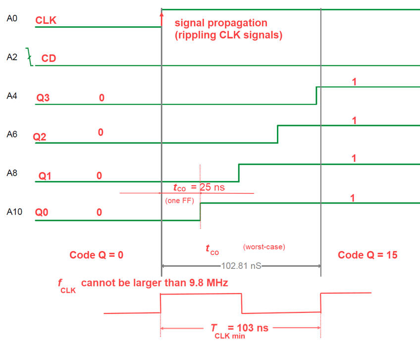
As represented in Fig. 13, it is possible to zoom (for instance triggering capture when Q3 has a rising edge) at a given transition to measure the propagation delay CLK to output (tCO) observing at the same time the asynchronicity due to the chain of CLK signals. Use resolution and zoom instrument knots to capture signals at the range of ns.
 |
|
Fig. 13. Zoom at a given signal transition, where all the output values are switching. Use the display scale and the capture resolution knots for adjusting the waveforms. |
4. Test
As we do when analysing circuits, a good way to check results is to compare them with results from other analysis methods. They must match if evething is correct. Discuss your solutions and methods with other team mates.
5. Reporting
Sections (1) + (2) + (3) + (4) (at least four sheets of paper). Follow this rubric for writing reports.
|
Laboratory |
Lab 5: Analysis of circuits based on flip-flops: method I, method II, method III prototype Method III: VHDL synthesis and simulation analysis. Analysis of the propagation delay CLK to output (tCO) using gate-level simulations |
[10/4] |
2.3.7.3. Method III: Using VHDL tools (plan C2 circuit)
1. Analysis specifications
Method III: Capture the circuit in Fig. 1 in VHDL as a plan C2 structure, synthesise it and run a testbench simulation to represent all inputs and outputs in time in a waveform logic diagram. How many states does the circuit have? What is the application of this circuit and the output codes?
|
|
Fig. 1. Symbol and schematic of the asynchronous circuit to be analysed. CLK is a rectangular wave of TCLK period. Clear direct (CD) is a single pulse any time the user like to initialise the circuit. |
|
|
|
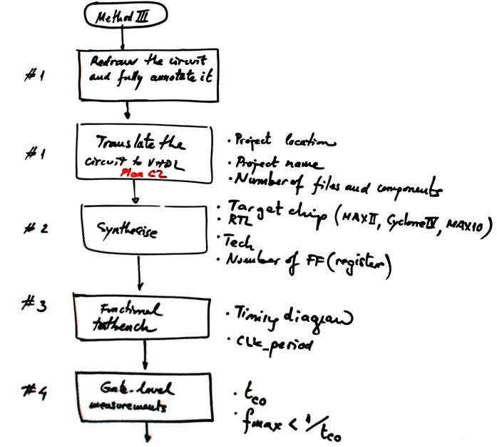
2. Planning
Using VHDL tools requires a sequence of steps, as shown in Fig. 2. The timing diaagram in step #4 can be compared to other methods.
 |
|
Fig. 2. Planning the solution using method III. |
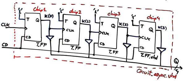
Step #1: Before using developing EDA VHDL tools, we need to translate the circuit schematic into VHDL. Fig. 3 is the circuit redrawn with all the items, signals, components and ports annotated. This is a plan C2 project consisting of two files.
 |
|
Fig. 3. Circuit fully annotated and ready for translation to VHDL. |
Translate the schematic into VHDL and find project components.
Step #2: Run the synthesis of the circuit in a programmable chip.
CPLD or FPGA target chip options:
option #1: MAX II
option #2: Cyclone IV
option #3: MAX10 (This chip does not allow real gate-level simulations, sdo files are not generated)
Step #3: Obtain the timing diagram running a testbench on functional simulations. From this solution, solve the questions in specifications.
Step #4: Additionally, gate-level simulations and timing analyser will allow the measurement of propagation delays. The key parameter is the propagation time from CLK to output (tCO) in a given transition.
Measure the circuit maximum speed using gate-level simulations tool (because of the many CLK's Quartus Prime timing analyser is not convenient in this type of asynchronous circuits).
Pictures, notes, scanned materials, theory and all VHDL project files can be stored in this project location:
C:\CSD\P5\Circuit_async\VHDL\(files)
3. Development
Step #1: Write down the VHDL file corresponding the Circuit_async.vhd from the schematic above in Fig. 3. The flip-flop description in VHDL is available in its tutorial T_FF. The other flip-flop types are JK_FF, D_FF.
Step #2: Start a synthesis project Circuit_Async_prj in Quartus Prime for a given target chip.
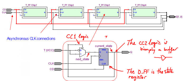
Synthesise the circuit and check the number of registers (flip-flops) used.
Print the RTL schematic and discuss it.
 |
|
Fig. 4. RTL produced by the synthesiser. |
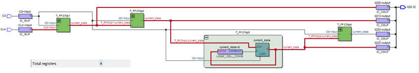
Print the technology schematic and discuss it. How many resources are used (logic cells and registers)?
 |
|
Fig. 5. Technology schematic to be tested using gate-level simulations. In red is represented the CLK path from one T_FF to the next. Note how four D_FF registers are used, one per T_FF. |
Step #3: Generate a testbench driving CLK and input signals (in this case the CD pulse). Two processes
Fig. 6 shows the generalised VHDL testbench schematic that we have in mind to run simulations for our sequential systems under test. Remark the significant change replacing Min_Pulse constant by CLK_Period to define from now on time resolution.
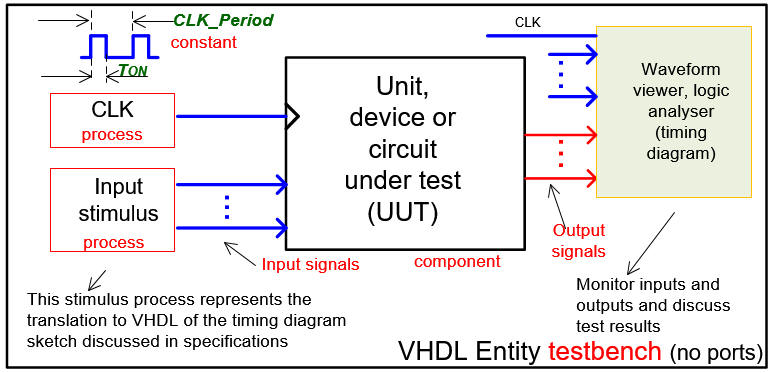 |
|
Fig. 6. General testbench fixture for sequential systems, including at least two stimulus processes: one for the CLK and another for the remaining input ports. |
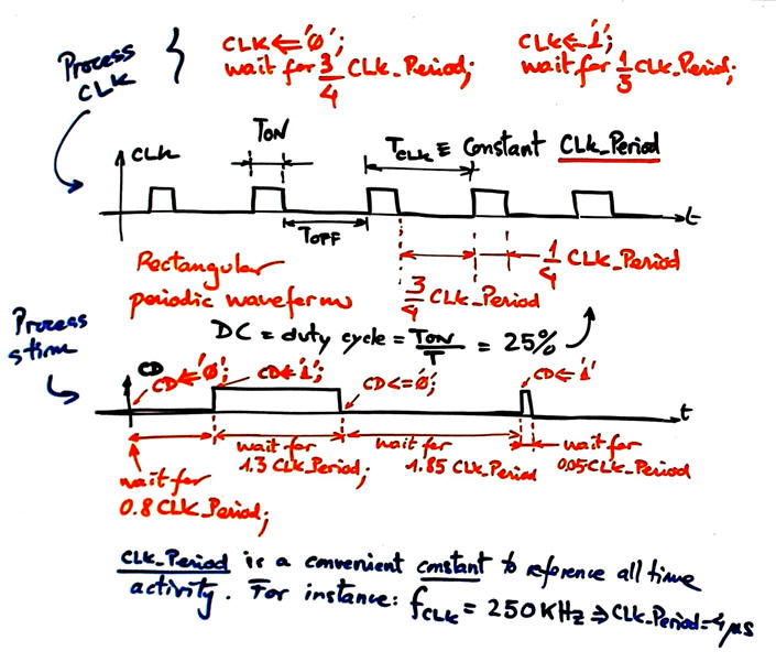
Fig. 7 represents the inputs required in this experiment. A periodic CLK waveform of rectangular shape, for instance with a duty cycle = 25% and a clear direct CD pulse that can be repeated when necessary to initialise again the circuit. Make all the timing relative to the constant CLK_Period, that is the equivalent in Chapter 2 to the Chapter 1 constant Min_Pulse.
 |
|
Fig. 7. CLK and CD activity to be described in the testbench processes. From this activity the simulator will calculate outputs. Normal operation of the circuit can be inspected for example setting CLK_Period = 4 us. And detailed time measurements on signal transitions can be performed setting CLK_Period = 40 ns when testing the real technology view synthesised circuit for a given target chip (FPGA or CPLD). |
This is an example testbench file Circuit_async_tb.vhd where to see how the CLK_Period constant is specified and how signal activity (and the CLK generation) is translated into VHDL processes.
Start a new functional ModelSim simulation.
Run the EDA VHDL tool and demonstrate how the circuit works adding comments to the printed sheet of paper containing the waveforms.
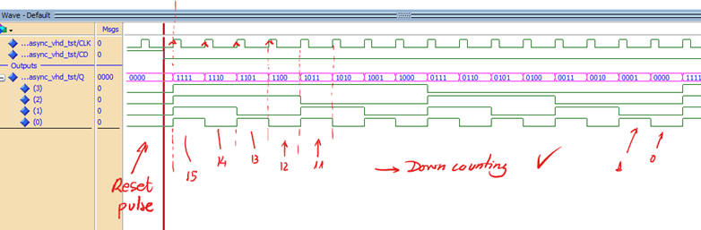 |
|
Fig. 8. Waveforms from functional simulation. |
Questions solving and discussion. This circuit is acting as a 4-bit binary counter in radix-2.
Step #4: Start a new ModelSim gate-level simulation using the same testbench.
Run the EDA VHDL tool using the same testbench in order to measure the CLK to output propagation delays (tCO). You can also calculate the maximum frequency of operation.
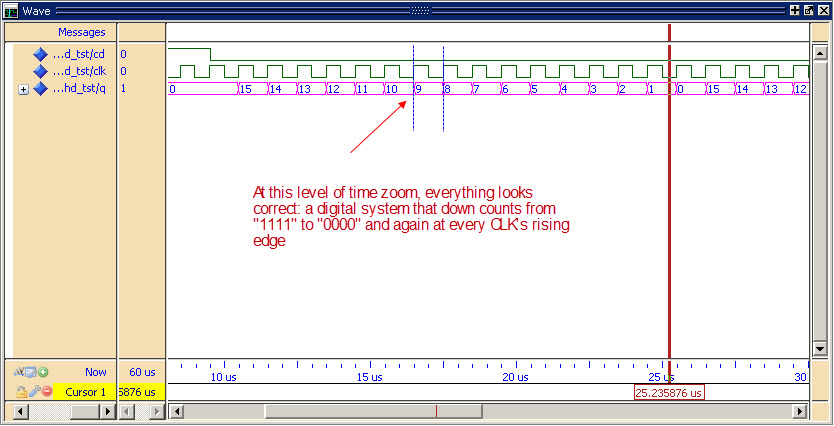 |
Fig. 9. Results from a gate-level simulation zooming all the test time to see that it works as expected, like the functional simulation. |
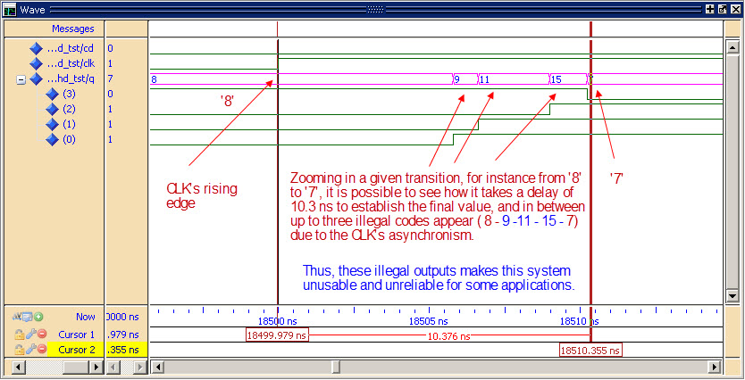 |
Fig. 10. Results from a gate-level simulation focusing a single transition in ns time resolution window. |
Measurements and question solving. What is the maximum speed of operation?
What about the timing analyser tool? Is it easy to use and obtain results in such circuits with several CLK signals?
4. Test
Compare results with other analysis methods. For instance, Fig. 13, Fig. 6 and Fig. 3 are giving the same outputs: down counting continuously "1111", "1110", ..., "0000", "1111", ...
Extra optional (recommended): enhance the circuit in Fig. 1 as shown in Fig. 11 adding a decoder Dec_4_16 to convert 4-bit radix-2 output codes to 16-bit one-hot codes for better observing how poorly is performing in transitions from one code to the next. The point here is to see the drawbacks of such asynchronous circuits with respect to synchronous designs based on finite state machines (FSM) to be studied in the next P6.
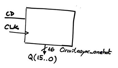 |
Fig. 11. Symbol of the modified circuit with 16-bit one-hot vector output Q(15..0). Only one output must be high at a time. |
In this way, it is even easier to visualise the problems at CLK transitions of this circuit. Project location at:
C:\CSD\P5\Circuit_async_onehot\(files)
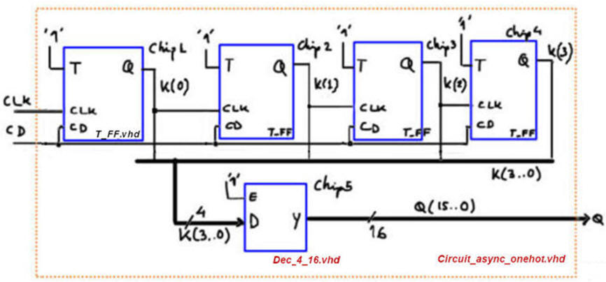 |
Fig. 12. Schematic of the asynchronous circuit with one-hot outputs designed to observe the poor performance of asynchronous circuits based on CLK rippling or using CLK as another logic signal to control flip-flops. |
The VHDL description of the decoder component is found in Dec_4_16 tutorial eample page. Thus, the project resulting from the translation of Fig. 12 schematic Circuit_async_onehot.vhd will generate one-hot outputs.
 |
|
Fig. 13. RTL produced by the synthesiser of the project with one-hot outputs. |
Similar waveforms in the logic analyser can be observed running Counter_onehot_16bit_async using a similar testbench Circuit_async_onehot_tb.vhd.
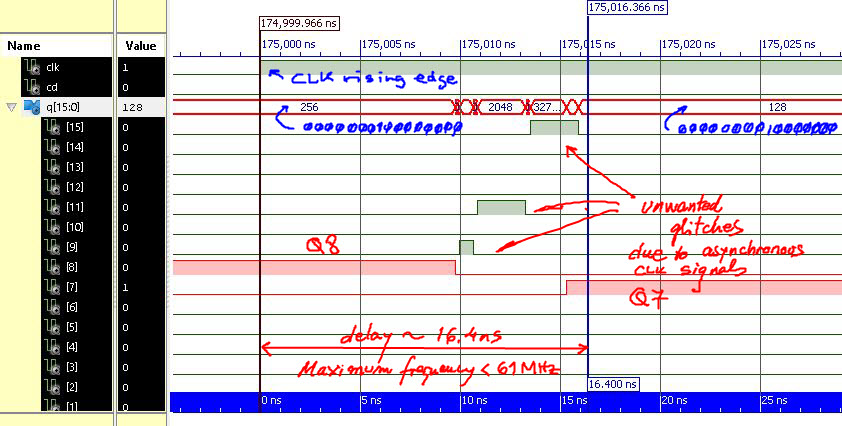 |
Fig. 14. Results from a gate-level simulation focusing a single transition in the Circuit_async_onehot. |
Optional. Compare Fig. 14 with gate-level results from a canonical FSM-based synchronous design of a 4-bit binary down counter (glitch, propagation time, etc.).
|
Laboratory |
Lab 5: Analysis of circuits based on flip-flops: method I, method II, method III, prototype [P5] Circuit based on FF prototype and measurements |
[10/4] |
5. Prototyping
Here in this section we can continue the project demonstrating how this Circuit_async can be implemented in the MAX10 Lite board. This project will be named Circuit_async_top and located at:
C:\CSD\P5\Circuit_async\Circuit_async_MAX10\(files)
Sereval options and features will be included in the prototype:
- CLK source : external push-button or inernal crystal oscillator
- Oscillator frequency : 10 Hz or 1 Hz.
- Output code represented using 7-segment displays: BCD or HEX
- Dec_4_16 outputs represented in unused segment
- Binary radix-2 output code from the Circuit_async in LED
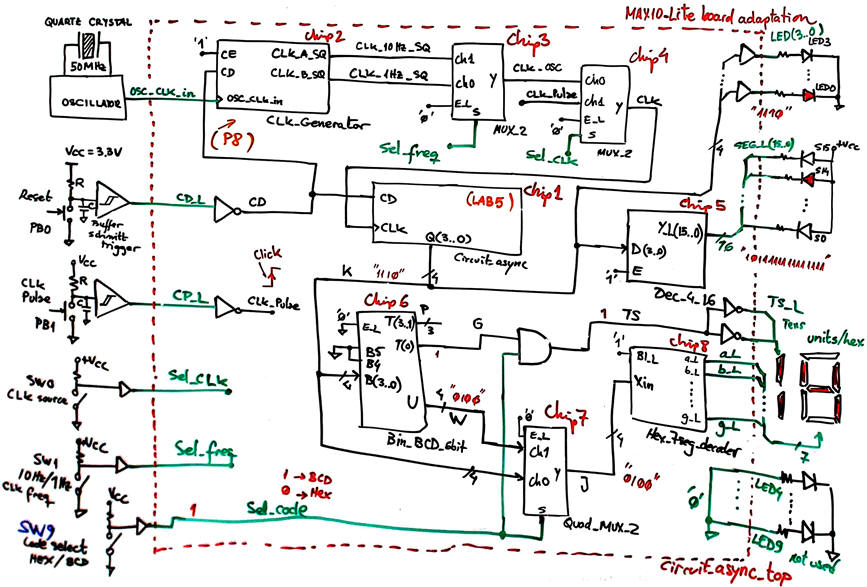 |
Fig. 15. Adaptation to the MAX10-Lite board. |
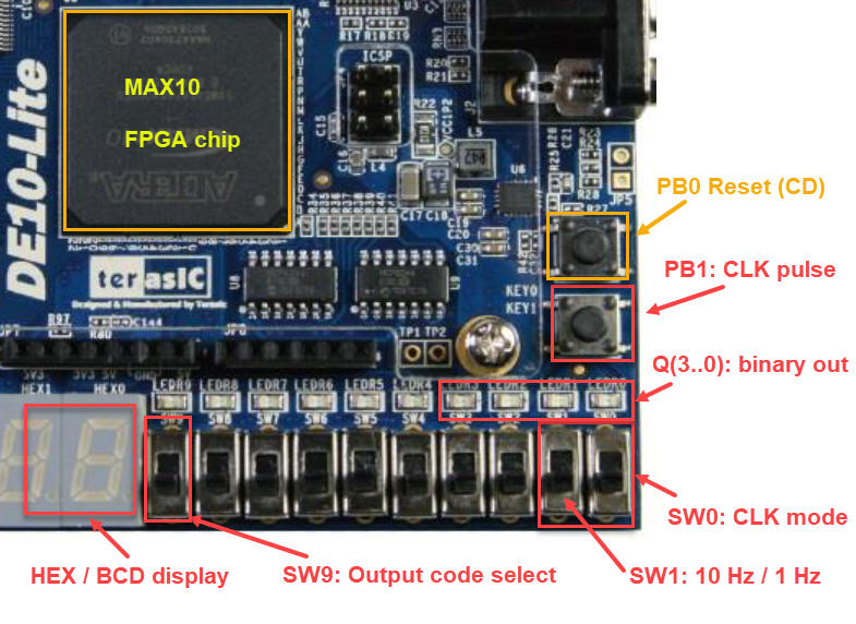 |
Fig. 16. Picture of the push-buttons, switches, LED and segments used. |
 |
Fig. 17. Details on the assignment of some free LED segments to the Dec_4_16 outputs. |
The full project zipped as Circuit_async_top.zip.
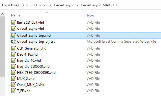 |
Fig. 18. List of VHDL files included in this structured plan C2 hierarchical project. |
The spreadsheet containing the list of pins used is in this file Circuit_async_top_prj.csv. It can be imported into the Pin pLanner tool as represented in Fig. 19.
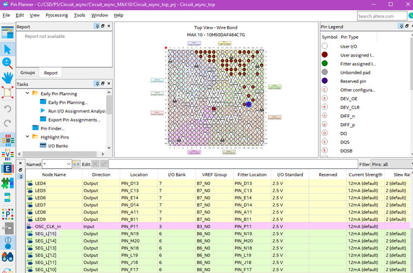 |
Fig. 19. Pin planner application where FPGA pin can be assignmed to inputs and outputs using the MAX10-Lite user manual. |
Using the programmer tool as shown in Fig. 20, we can configure the FPGA to run this application. The configuration file is named: Circuit_async_top.sof. When this file is available, the programmer tool can be used directly from the operating system.
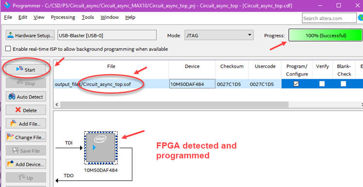 |
Fig. 20. Programmer tool. |
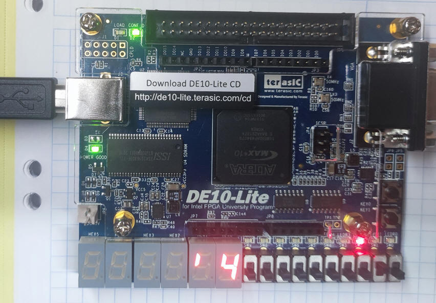 |
Fig. 21. Picture of the board running. |
- What is the problem when using the push-button PB1 CLK_pulse to generate rising edges for the circuit's CLK? How this problem can be solved?
This is the project solution Circuit_async_MAX10_d.zip. A new CLK_200Hz_SQ signal generated by the CLK_Generator is driving the debouncing filter that cleans the noisy CP_L from PB1 push-button. In this way the bouncing noise generating when clicking and releasing keys is filtered and thus the signal CLK_pulse becomes is a single and clean digital pulse.
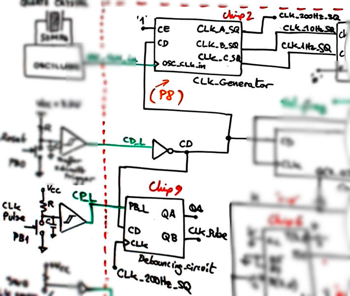 |
Fig. 22. Debouncing the external CLK signal from the PB1 CP_L. |
6. Reporting
Follow this rubric for writing reports. Sections (1) + (2) + (3) + (4) (at least four sheets of paper).
Books and internet references
This All About Circuits article (be aware that the naming conventions and procedures are different) is adequate to examine in detail the problem of asynchronous circuits like this one analysed in this lab project based on rippling CLK signals through a series of flip-flops.
| Home Term 24/25-Q1 Contact Products Electronic devices and companies Software Books Magazines Instruments DEE Library EETAC DEEL |

|
|
| Web activa des de 09/2001, @ F. J. Robert, J. Jordana. Web editat amb Microsoft Expression Web 4. El contingut és un complement als materials d'estudi del curs Circuits i Sistemes Digitals disponibles al campus digital Atenea. Llicència:Reconeixement 4.0 Internacional de Creative Commons |