|
|
Bachelor's Degree in Telecommunications Systems and in Network Engineering |
|
| | ||
PLA5: Analysing circuits based on 1-bit memory cells (flip-flops) |
||
| NOTE: This post lab assignment must be solved only after having completed successfully lab session Lab5 because you will repeat procedures and adapt materials from it. |
Specifications
Analyse using method I the proposed circuit. This means finding how the circuit works in time once initialised and what outputs are generated.
Check results using method II or method III, your instructor will tell you which is your individual assignment.
In this PLA you will solve two independent analysis projects the results of which can be compared and has to be the same.
| Example of individual assignments | ||||
| Project number | Circuit entity | Method for checking results | VHDL target chip for synthesis or technology modelled in Proteus | |
| Student 1 | A2.4 | Circuit_I | 2 | CMOS 4000 library |
| Student 2 | A2.5 | Circuit_F | 3 | Cyclone IV |
| Student 3 | A2.9 | Circuit_H | 2 | LS-TTL library |
| Student 4 | A2.4 | Circuit_I | 3 | MAX II |
| ... | ... | ... | ... | ... |
It is a new chapter, with a new component:1-bit memory cells. Thus, by means of P5-LAB5-PLA5 we try to study in detail at least the following goals:
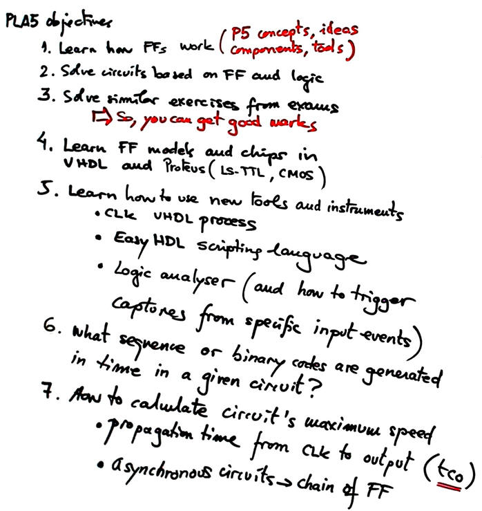
These new devices are complicated, because current values determine the new states. In this way, we better go step by step; we need to be sure that the concepts are clearly comprehended before dealing with more complex circuits. Discuss all your doubts with your team mates and instructors.
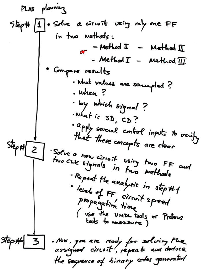
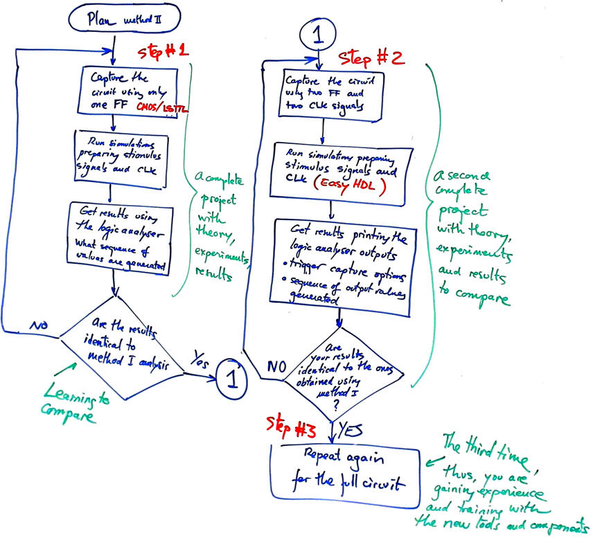
The flowchart below is an example of analysing your circuit using method II. The idea of subdividing the task into several steps and NOT advancing until the step is complete, is mandatory and similar for the three analisis methods. It is the best way to learn correctly the new tools, procedures and how the new clocked components works.
| Home Term 24/25-Q1 Contact Products Electronic devices and companies Software Books Magazines Instruments DEE Library EETAC DEEL |

|
|
| Web activa des de 09/2001, @ F. J. Robert, J. Jordana. Web editat amb Microsoft Expression Web 4. El contingut és un complement als materials d'estudi del curs Circuits i Sistemes Digitals disponibles al campus digital Atenea. Llicència:Reconeixement 4.0 Internacional de Creative Commons |