|
|
Bachelor's Degree in Telecommunications Systems and in Network Engineering |
|
|
|
||
|
|
Dec_4_16: behavioural single-file VHDL (flat) plan B |
|
|
|
||
Binary decoder from 4 to 16
1.Specifications
Design a binary decoder 4 to 16 active-high (Dec_4_16) following plan B based on the behavioural description of the truth table. Theory on decoders is introduced in L2.3. A similar commercial chip with active-low outptus is the 74HCT154.
Fig 1 shows the circuit symbol and truth table. When the chip is enabled, output vector Y(15..0) may be considered as coded in one-hot.
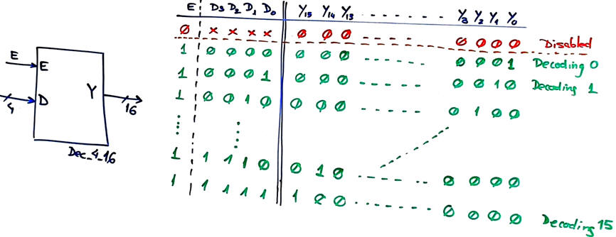 |
| Fig. 1. Dec_4_16 symbol and truth table considering active-high inputs and outputs. |
Fig. 2 shows an example of timing diagram where the Min_Pulse duration is also defined as a constant for representing time.
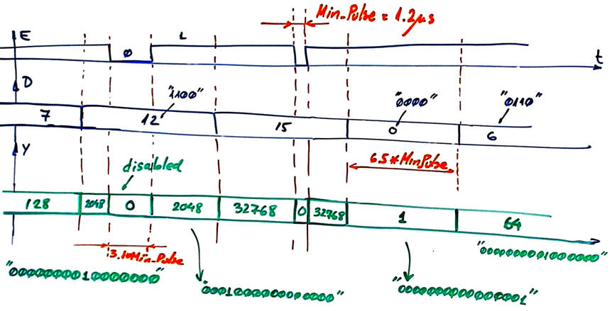 |
Fig. 2. Example of a timing diagram showing some input activity. Later on, in design step 4, this timing diagram will be translated into a VHDL testbench as the stimulus process to run simulations. |
2. Planning
This is a mind map represesenting our VHDL design flow and the main concepts involved in designing combinational circuits.
For plan B, as shown in Fig. 3, we can represent a schematic to capture the complete truth table using signals and buffered inputs ports.
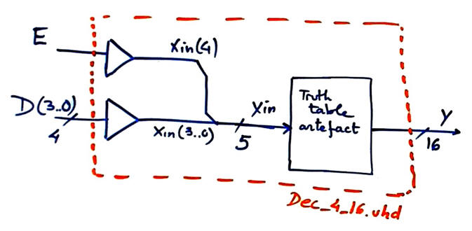 |
Fig. 3. Example schematic based on the truth table artefact. |
Project location:
C: \CSD\P2\Dec_4_16B\(files)
3. Development
1.- Write down the VHDL file translating the schematic above in Fig. 3. This Dec_4_16.vhd is an example translation.
2.- Start an EDA tool project Dec_4_16_prj for a CPLD/FPGA target chip and obtain the synthesised circuit. Represent and analyse the RTL and technology views.
3.- Examine and print a commented copy of the RTL schematic. In Fig. 4 is represented an example of RTL and technology schematics synthesised by the computer tool Quartus Prime.
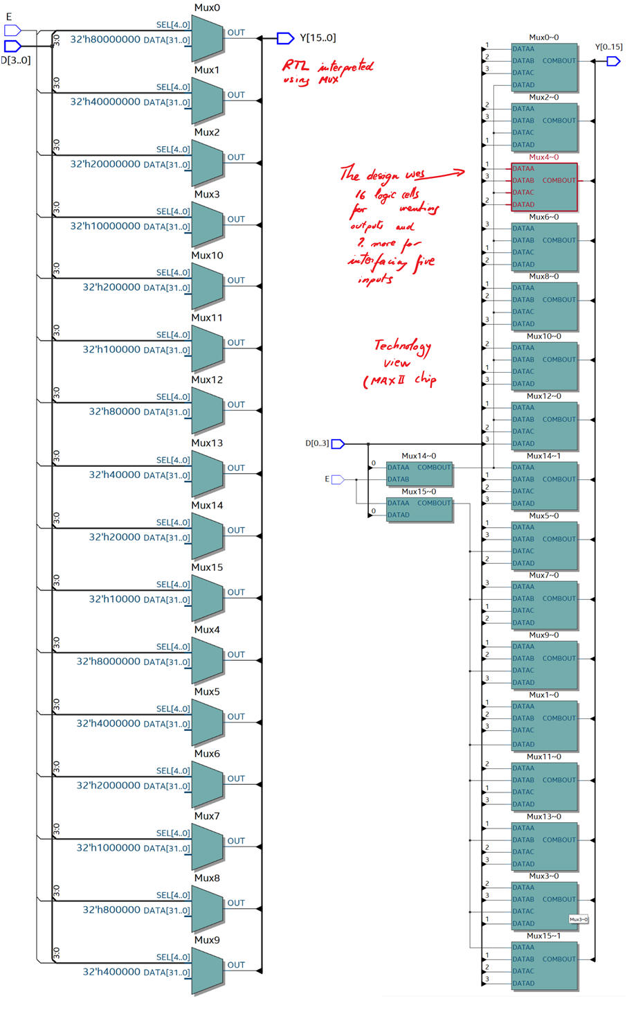 |
Fig. 4. This is the RTL and technology views for an Intel MAX II target chip. |
4. Testing
1.- Start an EDA VHDL simulator project and verify the Device-Under-Test (DUT) using a VHDL simulator test bench (Dec_4_16_tb.vhd).
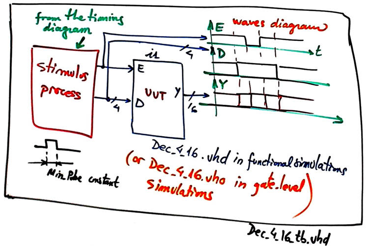 |
Fig. 5. Testbench fixture for applying stimulus vectors to the unit under test. |
2.- Verify applying sufficient test vector that the device works as expected (verify the truth table). Print timing diagram screen and add comments on the signals to show how the device works.
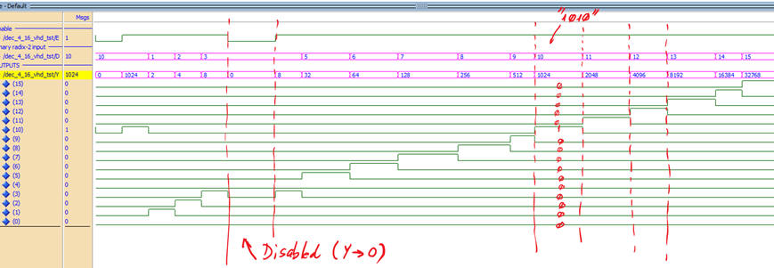 |
Fig. 6. Example of timing diagram from ModelSim wave. The device works as expected. |
5. Report
Project report starting with the template sheets of paper, scanned figures, file listings, docx , pptx, or any other resources
6. Prototyping
Use training boards and perform laboratory measurements to verify how the circuit works for real.
| Home Term 26/27-Q1 Contact Products Electronic devices and companies Software Books Magazines Instruments DEE Library EETAC DEEL |

|
|
| Web activa des de 09/2001, @ F. J. Robert, Web editat amb Microsoft Expression Web 4. El contingut és un complement als materials d'estudi del curs Circuits i Sistemes Digitals disponibles al campus digital Atenea. Llicència:Reconeixement 4.0 Internacional de Creative Commons |