|
|
Bachelor's Degree in Telecommunications Systems and in Network Engineering |
|
| Analysis and design tutorials | Analysis and design assignments | Prototypes | Exam 1 | Exam 2 | Questions and assessment |
CSD EXA1: midterm exam examples and solution ideas |
2526Q1
Problem 1
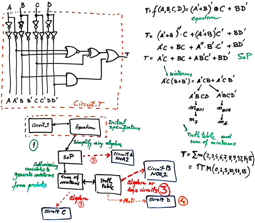
1. Method I consist of using algebra to simplify towards a regular SoP or PoS. Then we can add the missing variables to generate minterms from each product. You can use method II to check your solutions "Circuit_T.pdsprj" .
2. We observe that the longest propagation path is from input B to output T: NGL = 5.
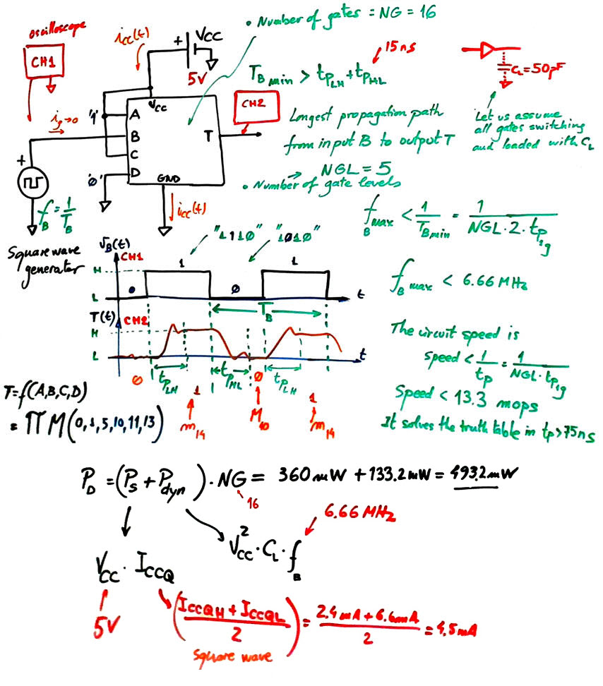
Therefore, we can calculate the power consumption of the circuit operating at the maximum frequency. We will assume that all the circuit gates are switching and they are half period high and half period low (LS-TTL has different quiescent current consumption when high and low).
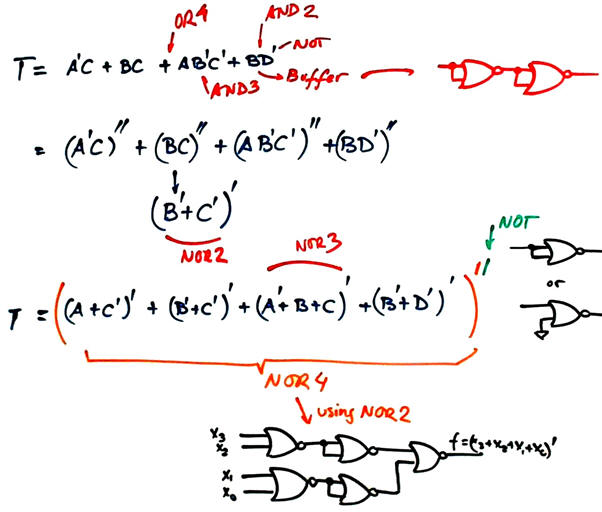
3. From our plan above, you can generate several only-NOR2 circuits. One way is to use the SoP (Circuit_A); another way is to use the sum of minterms (Circuit_B) or even from the product of maxterms (Circuit_C). You can even consider the circuit in Fig. 1 and transform it gate by gate.
For instance the Circuit_A from SoP is deduced as:
4. From the truth table or the canonical expressions we can apply the MoD covered in in lecture L3.3, as shown in the plan (Circuit_D).
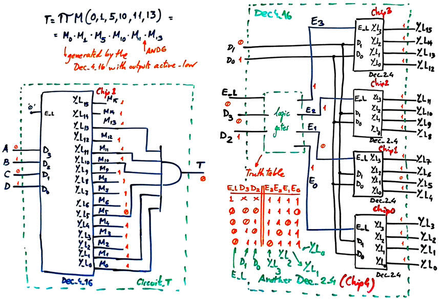
And the circuit expansion concept proposed as a plan C2 application, covered in our mind map (L2.1) can be used for inventing the Dec_4_16 required in this application, using smaller Dec_2_4 of the same kind. In the picture, a Dec_4_16 with active-low outputs capable of representing all the maxterms is represented.
Problem 2
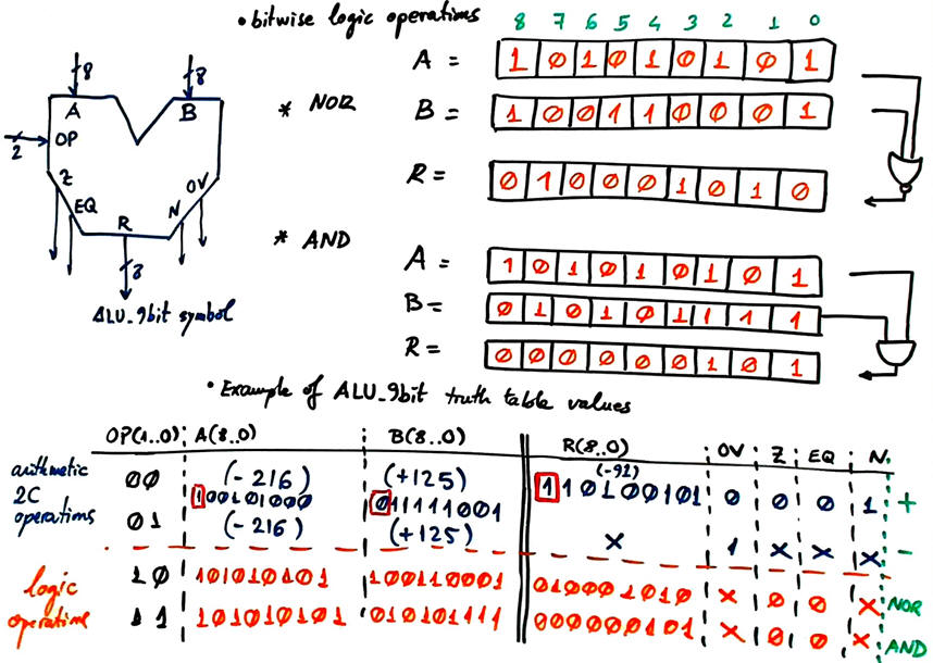
1. and 2. First, solve the examples of arithmetic operations in L4.1, and also the examples on logic operations in L4.2. Then, repeat for the given operations in this problem.
NOTES:
-
Be aware of the sign bit position when performing arithmetic operations in 2C to avoid errors; use a coloured square to indicated them, as we do all the time in CSD.
-
Cout signal from the internal component Adder_9bit is not the OV flag; it may be inferred from OV = C8 xor Cout as demonstrated in P4.
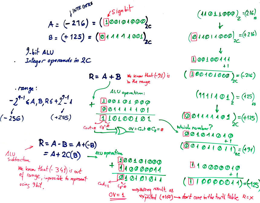
Another way to practise with numbers and operations is to solve the pre-lab activity PA1 in LAB4.2.
Problem 3
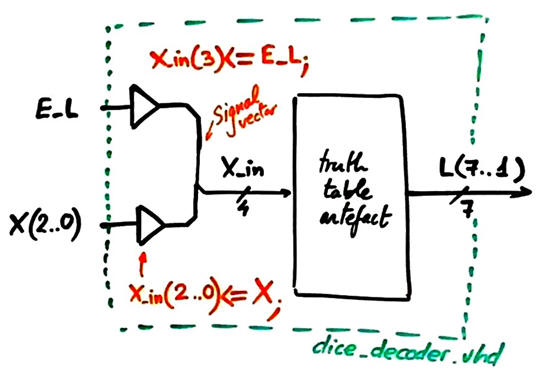
1. This is the Proteus "dice_decoder.pdsprj" circuit capture in case you like to experiment with the circuit. This is the "dice_decoder.tbl" for Minilog in case that PoS or PoS equations were required. In this problem we will work directly with the truth table and its canonical representations. The picture below shows the sum of minterms.
2. The LED are connected active-high, thus the worst-case scenario is when a gate generates VOHmin = 2.7 V as the high voltage ('1'). In this situation we still require to drive the LED with IDQ = 600 µA.
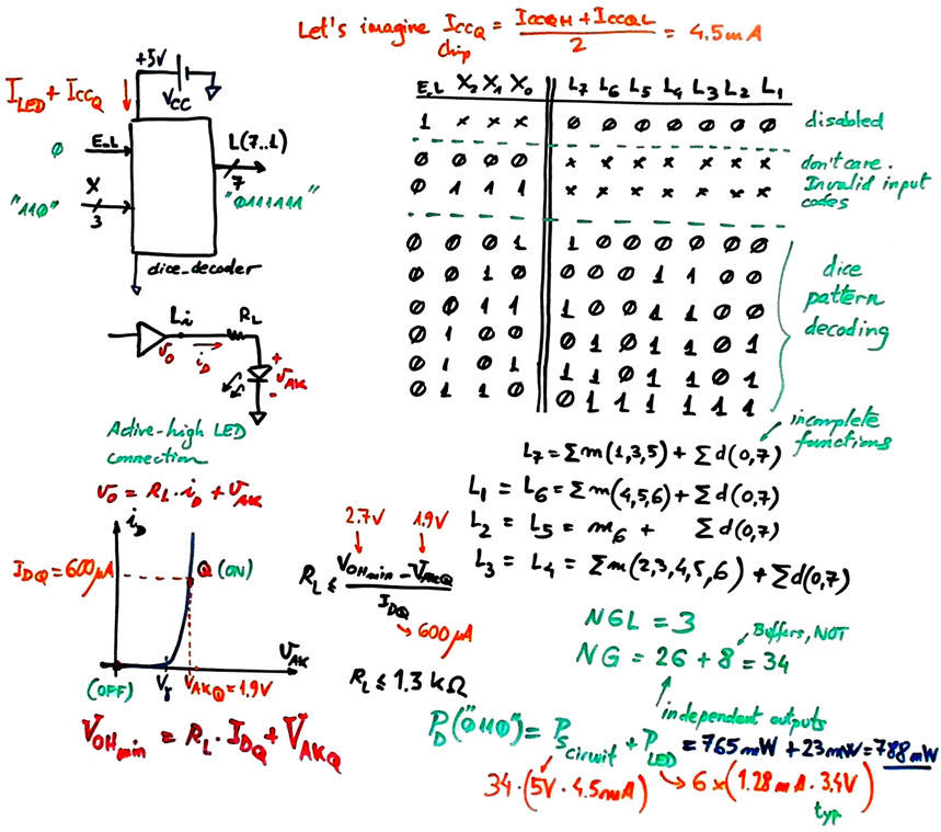
There is another situation that we may consider: is it really possible to bias a LED with IDQ = 600 µA supplied from an LS-TTL gate? The datasheet indicates that a gate can only drive IOHmax = - 400 µA. Consequently, the LED circuit should be driven by active-low outputs because the maximum output sink current is IOLmax = 8 mA. We can try to simulate these assumptions or we can experiment and measure using a prototype.
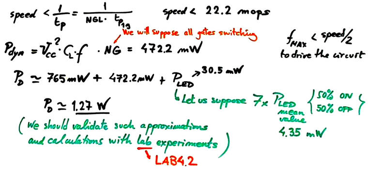
3. Supposing independent outputs, each output will be implemented in three gate levels: NGL = 3. We can drive the circuit with vectors switching at fMAX < 11.1 MHz. The circuit's power consumption is much larger when switching at high frequencies, as explained in lecture L4.3.
4. Using plan B we can translate the full table in a single file.
Min_pulse > tP = 45 ns The minimum Min_Pulse for ModelSim gate-level simulations has to be larger than the circuit's propagation time to allow signal propagation and the generation of stable output logic levels.
| Home Term 26/27-Q1 Contact Products Electronic devices and companies Software Books Magazines Instruments DEE Library EETAC DEEL |

|
|
| Web activa des de 09/2001, @ F. J. Robert, Web editat amb Microsoft Expression Web 4. El contingut és un complement als materials d'estudi del curs Circuits i Sistemes Digitals disponibles al campus digital Atenea. Llicència:Reconeixement 4.0 Internacional de Creative Commons |