Chapter 2 problems |
- D2.9 - |
Water tank controller (FPGA-VHDL) |
1. Specifications
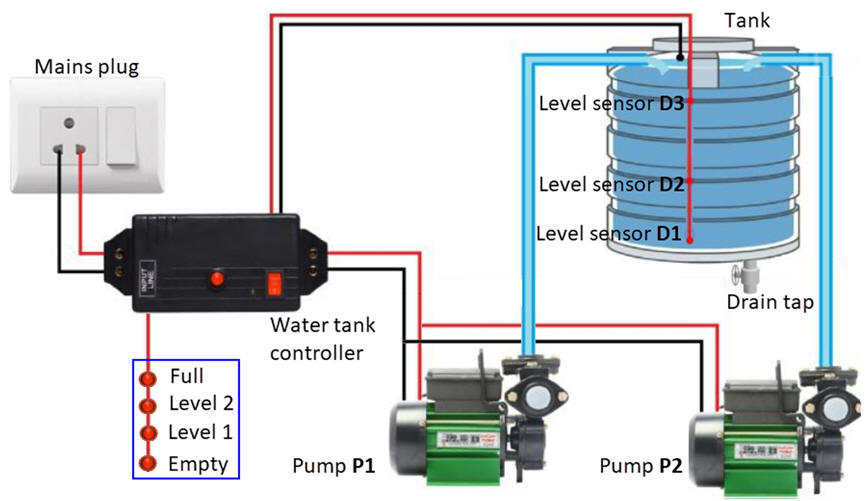
We want to design a water tank controller (Tank_cntl_top) as an application of FSM that can drive two pumps independently, as represented in Fig. 1. The tank has level sensors D1, D2, and D3 attached to the wall, so that a '1' is generated when the sensor is sunk into water. The controller works as follows: when the tank is empty, below D1, both pumps work simultaneously; when the water level is above D2 pump P1 stops; when the water is above D3, meaning that the tank is full, pump P2 stops; and finally, the pumps do not switch on until the water level is again below D1.
The same project designed programming a μC is in D3.9.
 |
|
Fig. 1. Diagram of the water tank installation. |
In addition to controlling the water level in the tank, we also want to indicate in a LED column and using a 7-segment digit the current level of the water in the tank. We can even add a tap valve to stop water drain when certain low level is reached.
In a new design phase we will include a real-time clock to measure how long does it take to empty the tank once full and the tap turns on.
2. Planning
Design phase #1: basic features. FSM architecture and current state encoding, asynchronous reset (CD), system clock (CLK), sampling input values, synchronous systems, maximum speed of operation, etc. Solve the circuit for the design step #1. This means covering P5 and P6 circuits, concepts and ideas.
Project location:
C:\CSD\P6\Tank_cntl\(files)
- Design step #1. Consider an initial circuit only with the tank sensors, the pump outputs and the 4-LED column.
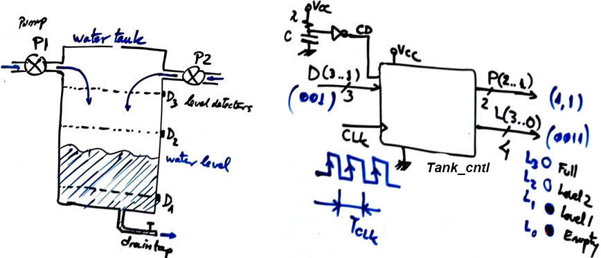
Fig. shows an sketch of the system and its symbol.
 |
|
Fig. 2. Tank sketch and first idea of the symbol. We can use a 1.25 kHz CLK signal to synchronise the machine. |
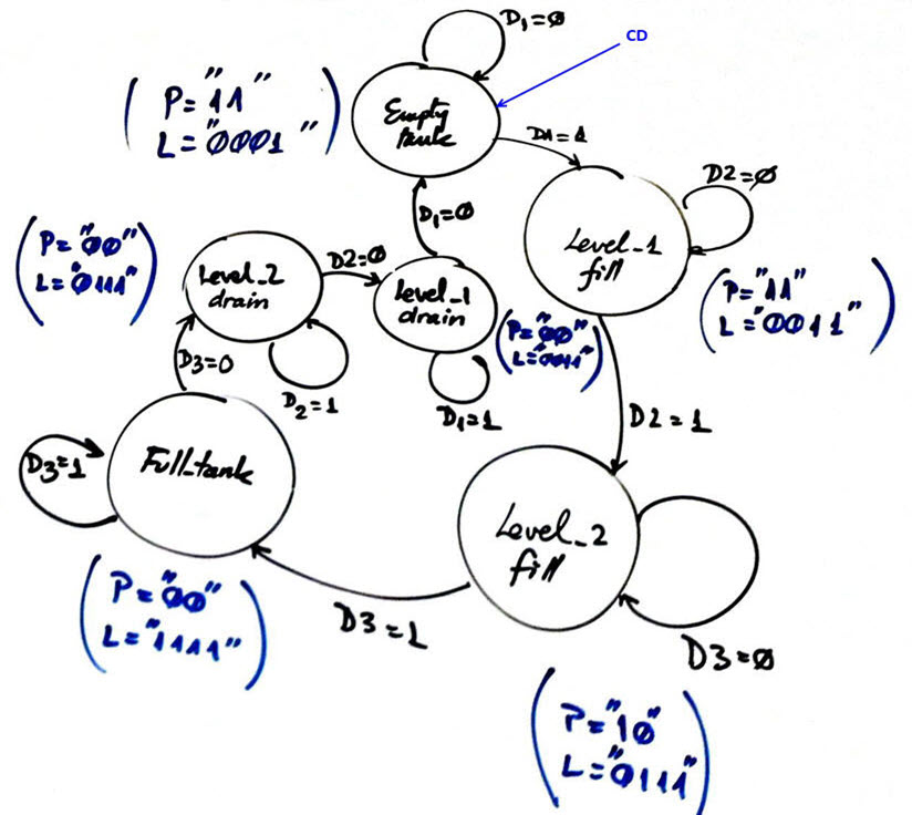
Draw the FSM state diagram. Fig. 3 shows an example of the many possible, where up to six states can be identified to memorise the water level and pump actions.
 |
|
Fig. 3. State diagram example. |
Sketch a timing diagram showing the main operations and also imagining state values. These stimulus signals can be applied in section fourth in the testbench process translated to VHDL.
 |
|
Fig. 4. Timing diagram example. |
Adapt the FSM architecture to this problem, naming and connecting all signals and inputs and outputs. This will be translated as a single plan C1 VHDL file. Deduce how many D_FF are required when encoding FSM states using the following options and draw the state register memory:
Option #1: Radix-2 (sequential)
Option #2: Gray
Option #3: Johnson
Option #4: One-hot
 |
|
Fig. 5. FSM adaptation to the problem. |
Write the CC2 truth table to obtain the outputs of the circuit and its flowchart.
 |
|
Fig. 6. CC2 truth table and its equivalent plan B flowchart ready for VHDL translation. |
Design the CC1 truth table to obtain the next state to go and its flowchart.
 |
|
Fig. 7. CC1 truth table and its equivalent plan B flowchart ready for VHDL translation. |
3. Development
Write the VHDL file.
Start a Quartus Prime synthesis project for one of the following programmable target chips:
Option #1: Cyclone IV EP4CE115F29C7
Option #2: MAX II EPM2210F324C3
Option #3: MAX 10 10M50DAF484C7 (for gate-level simulations, choose one of the previous options)
Inspect and discuss the RTL and technology schematics. Check the number of D_FF.
 |
|
Fig. 8. RTL schematic generated by Quartus Prime and project summary where we can check the resources used and the number of D_FF. |
 |
|
Fig. 9. Technology view where we can indicate and count the number of D_FF of the state register. |
4. Testing functional
Draw the testbench fixture, add stimulus processes to the VHDL template and run the EDA simulation tool to verify your design. Discuss your results on the wave pictures.
 |
|
Fig. 10. Testbench fixture schematic for the basic FSM in step #1. |
 |
|
Fig. 11. Waveforms showing the full cycle of signals and internal states of the automata. |
5. Testing (gate-level)
Measure the maximum CLK frequency related to tCO that can be applied to your design considering your target chip.
 |
|
Fig.12. Example of gate-level simulation to measure the propagation time from CLK to output (tCO). |
- Design step #2. Add a 7-segment display level indicator. Add a tap valve.
Go ahead with the step #2 only when step #1 is fully tested working correctly.
The user wanted to add an extra circuit to translate the LED column code into a 7-segment display. Thus, an additional combinational circuit CC3 is required to meet this new specification. Let us solve the problem using the ROM method for implementing logic functions. The wiring in Fig. 2 shows the naming conventions for the vector HEX0_L(6..0) common anode in the DE2-115 board user guide page 36 (or the DE10-Lite). Discuss the size [2^n x m] of the ROM and add this circuit to your system.
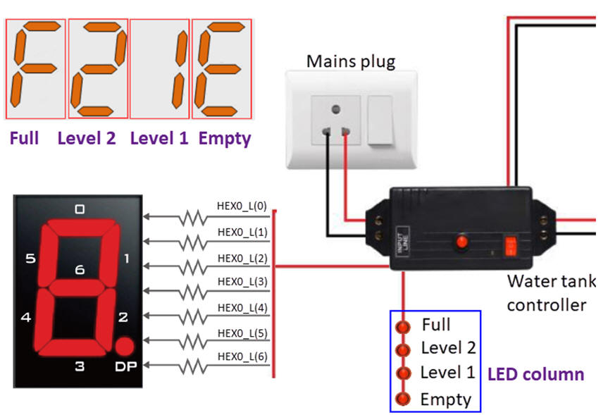 |
Fig. 13. Enhancement with a 7-segment display to display the symbols "F", "1", "2", and "E". |
Add a tap electric solenoid valve to switch off the water flow when the tank is below Level 1. Indicate this situation as well using a speaker driven by an audible 1.6 kHz tone waveform.
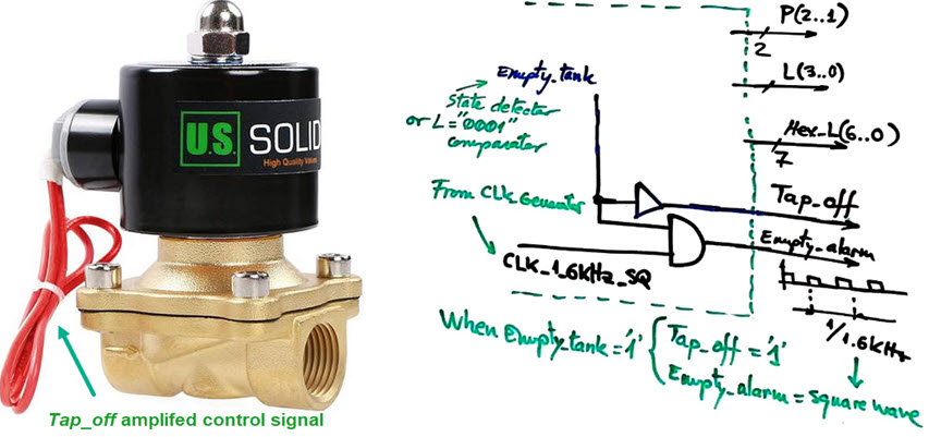 |
Fig. 14. Example of a commercial electric solenoid valve 220 V / 50 Hz and new output signals for controlling it and generating sound. |
What power driving circuits can be used to control the two 300W 220VAC/50Hz pumps and the tap solenoid valve? Design and model them in Proteus, similarly as it was proposed in LAB6.
In this way, we can suggest the internal architecture represented in Fig. 15 as a final circuit for this design phase #1.
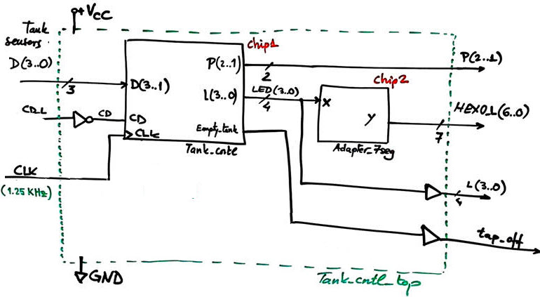 |
Fig. 15. Tank_cntl_top architecture proposed for design phase #1. Be aware that the Chip3 is designed in the next design phase. At this point you can simulate the two CLK signals required. |
Design phase #2: advanced features to measure how long does it takes to empty the tank.
Only when design phase #1 is fully tested working correctly and reported, solve the design phase #2 as advancing to cover P7 and P8 materials.
- Design step #1: Design a CLK generator to obtain all the necessary clocking signals from the 50 MHz target board quartz crystal oscillator. Deduce the number of D_FF required for this subcircuit.
Project location:
C:\CSD\P8\Tank_cntl_top\(files)
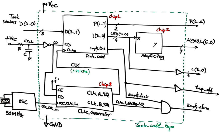 |
Fig. 16. Tank_cntl_top architecture proposed for design phase #1. Be aware that the Chip3 is designed in the next design phase. At this point you can simulate the two CLK signals required. |
Our aim is to measure how long does it take to empty the tank. Therefore, in two steps we can build the chronometer and connect it to our tank controller.
- Design step #2. Datapath for counting real-time. Design a Chronometer for minutes, seconds and tenths of a second (MM:SS:T) that uses two push-buttons to operate it: Start (ST) enables counting real-time and stop button (SP) is used for holding the time elapsed until another ST click is detected. Users visualise the current time display.
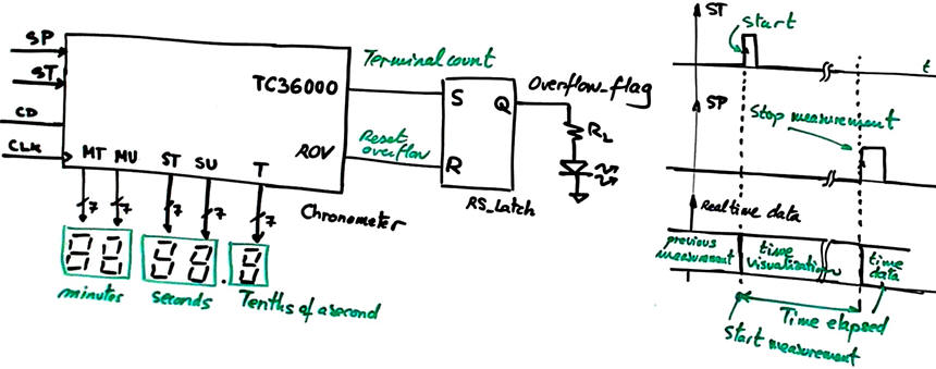 |
Fig. 17. Chronometer symbol and operation. |
For the Chronometer we can think easily on two options: (1) a chain of two digit BCD counters; or (2) a chain of binary counters modulo 60 and radix-2 to BCD code translators.
Project location:
C:\CSD\P7\Chronometer\(files)
- Design step #3. Complete the dedicated processor. Connect the Chronometer to the design phase #1 system, so that the clock starts when water flow is detected in the drain tap and stops when the empty signal D1 is detected. Search what kind of sensors can be used to detect water flow.
The FSM wil drive ST and SP pulses and the external RS_latch cell to set the overflow flag can be implemented alternativelly by the Tank_cntl FSM itself considering the terminal count as a status signal from this datapth.
Project location:
C:\CSD\P8\Tank_cntl_top\(files)
Hint: Suggested report organisation (similarly for slides presentation)
1. Specifications. First you explain all the specifications you like for your product. Add theory about anything of interest if necessary to comprehend the application.
2. Plan. Here you say that you have in mind several design phases and steps, each time incorporating only a few new features. And thus, that you simply will start developing and testing only what you have planned to be the first step.
3. Develop only the first step of the design phase #1
4. Test only the first step of the design phase #1
Annexes.
- Phase #1, step #2 (tab valve, empty alarm and additional display) Explain and do only what is modified in each of the previous sections to introduce the new features.
- Phase #2, step #1 (CLK_Generator) Explain and do only what is modified in each of the previous sections to introduce the new features. etc.


