|
|
Bachelor's Degree in Telecommunications Systems and in Network Engineering |
|
Chapter 2 problems |
- D2.5 - |
LED lamp dimmer (FPGA-VHDL) |
V1 |
1. Specifications (Version #1)
Luminaries work with high efficiency LED lamps and the light generated can be dimmed using a control circuit. A typical bulb is 12W, 12V, E27 screw fitting. To modulate the light intensity we can use simple pushbuttons or rotary knots.
The same project designed programming a μC is in D3.5.
  |
|
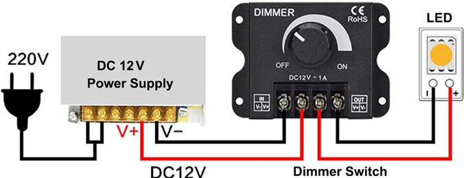
Fig. 1. Examples of luminaries, bulbs, dimmer circuits and power drivers. |
Let us propose the basic circuit for a dimmer in Fig. 2. Light intensity can be set in eight levels. Clicking active-low button up (UB_L) light intensity will increase, and clicking button down (DB_L) light will decrease. The idea behind controlling electrical power applied to a load like a LED bulb is to use digital pulsed width modulated waveforms (PWM). If the switching frequency is high, the eye will not be affected by flickering.
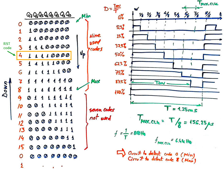
Let us invent a circuit capable of generating a PWM signal of fW = 800 Hz (T = 1.25 ms) (this waveform frequency will be an option) with duty cycle modulations (D %) of 0, 12.5, 25, 37.5, 50, 62.5, 75, 87.5, 100.
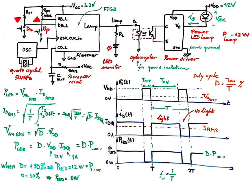 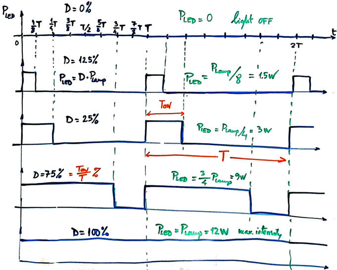 |
Fig. 2. Symbol and connection to a power lamp driver. Example of several PWM waveforms. |
The lamp power driver can be designed later using power MOS transistors or we can buy it along with the 3.3 V and 12 V power supply adapters. At this initial phase a simple standard LED can be used to monitor the light intensity or brightness generated at the Dimmer circuit Lamp output.
2. Planning
Better organise the design of a commercial product planning several phases and steps.
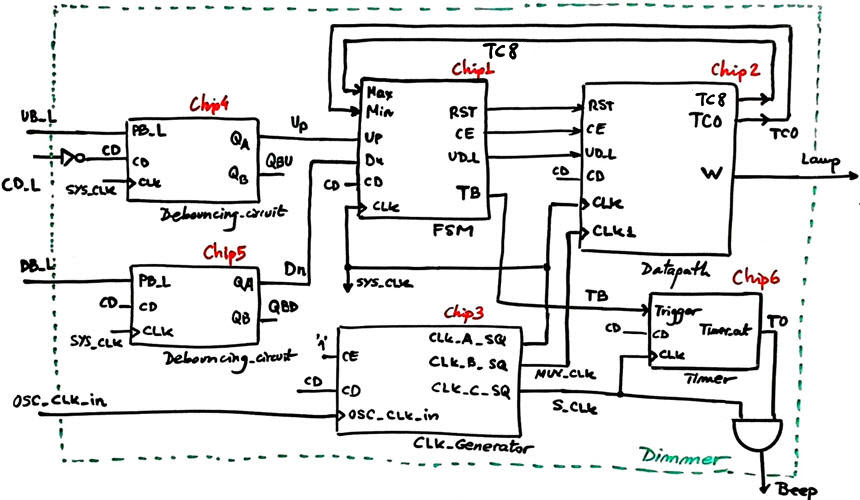
Design phase #1: Basic features: step #1: FSM, step #2: datapath and step #3: CLK_Generator
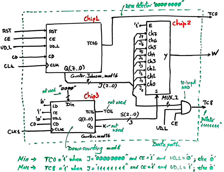
The top architecture for the project is the dedicated processor represented in Fig. 3.The control unit samples up and down light intensity push-buttons and generates control signals for the datapath.
Sampling buttons is carried out at the low frequency fSYS_CLK, for instance 200 Hz (the value to use is set as an option) as we did in other applications based on buttons and keys.
 |
|
Fig. 3. Example dedicated processor showing how several CLK frequencies are used for different functions. |
To control the FSM using clean and synchronised digital pulses we will add to each button a Debouncing_filter.
The datapath architecture is presented in Fig. 4. When clicking buttons, the FSM allows counting in Johnson up and down. This 8-bit Johnson code is multiplexed at fMUX_CLK by means of a 3-bit binary down-counter counter, thus producing a PWM Lamp waveform with period T (fMUX_CLK = 8· fW).
Let us solve this processor step by step.
- Design step #1. FSM
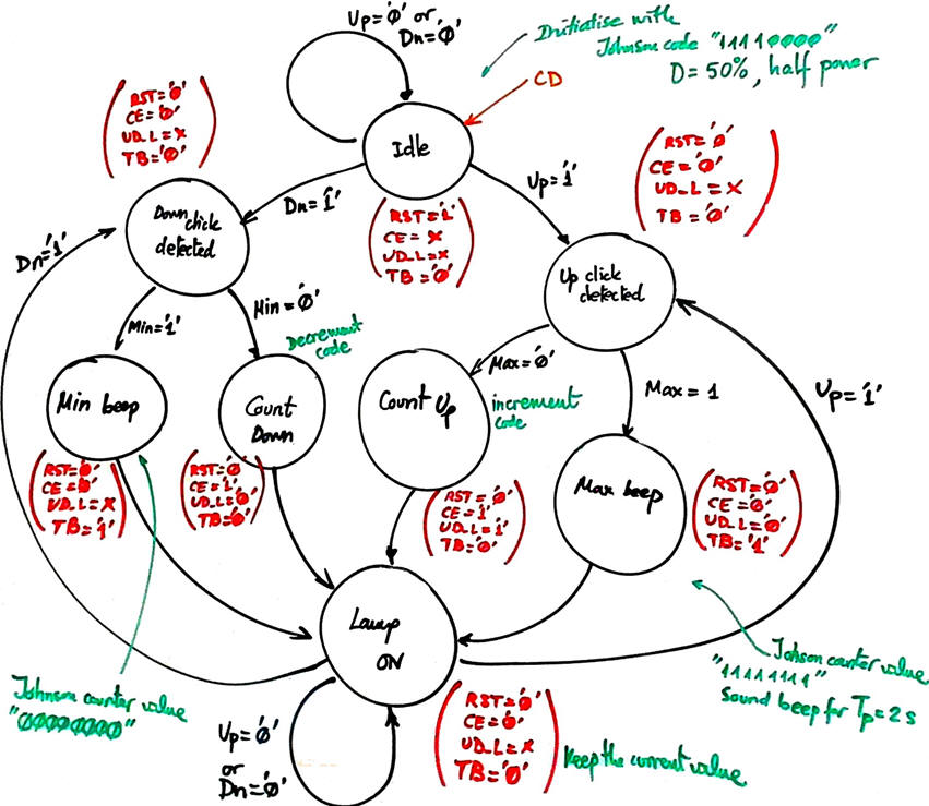
The FSM will run the state diagram below:
 |
|
Fig. 4. FSM state diagram. |
Adapt the FSM architecture to this problem, naming and connecting all signals and inputs and outputs.
Draw the state register memory and deduce the number of D_FF required when encoding the machine using one of the following options:
Option #1: radix-2 (sequential)
Option #2: Gray
Option #3: Johnson
Option #4: one-hot
Draw the CC2 truth table to obtain the circuit's outputs and its equivalent flowchart behavioural interpretation (plan B).
Draw the CC1 truth table to obtain the circuit's state transitions and its equivalent flowchart behavioural interpretation (plan B).
Project location:
C:\CSD\P6\dimmer\files)
Write the FSM VHDL file.
Start a Quartus Prime synthesis project for one of the following programmable target chips:
Option #1: Cyclone IV EP4CE115F29C7
Option #2: MAX II EPM2210F324C3
Option #3: MAX 10 10M50DAF484C7 (*)
(*) Remember that this chip does not generate "*.sdo" delay files, thus use another one when gate-level simulations are required.
Inspect and annotate the RTL and technology views. Check the number of D_FF synthesised in this application.
Generate a VHDL testbench fixture schematic. Translate the timing diagram sketch from the specifications into de corresponding stimulus processes.
Run functional simulations to verify your design. Visualise as well the internal states in the wave timing diagram.
Run gate-level simulations to measure the propagation time CLK to output (tCO). Measure the minimum TCLK period or the maximum frequency of operation of the FSM.
- Design step #2. Datapath
We use only nine Johnson codes of the sixteen available, hence, another feature to consider is disabling counting when reaching the minimum or maximum codes. We add to the system status signals to detect terminal counts Max and Min.
 |
|
Fig. 5. Datapath internal design based on using the Counter_Johnson_mod16. |
The MUX_8 is serialising continuously the current Johnson code to the output W.
 |
|
Fig. 6. Codes required at Chip2 MUX_8 input channels to serialise the output waveform. |
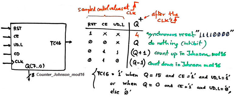
The key datapath component is the Counter_Johnson_mod16 with synchronous reset represented in Fig. 7. The RST signal is used to set half light power. We can implement it using one of the following three strategies:
Option #1: Johnson counter modulo 16 using plan C2 and the component Counter_mod16
Option #2: Johnson counter modulo 16 using plan Y.
Option #3: Johnson counter modulo 16 using plan C2 and the component Shift_reg_8bit.
 |
|
Fig. 7. Counter_Johnson_mod16 and its function table. |
Use the building block Counter_mod16 for implementing the Datapath Chip3 (it is used as a modulo 8 binary down counter modulo 8). It multiplexes Johnson codes and fixes the W output frequency. fW.
Project location:
C:\CSD\P7\dimmer\(files)
- Design step #3. CLK_Generator
Design the CLK generator circuit Chip3 in Fig. 3 from a 50 MHz quartz crystal oscillator to obtain all the clocking signals required to drive the application. Deduce the number of D_FF required for this component. Add this Chip3 to the top architecture.
 |
|
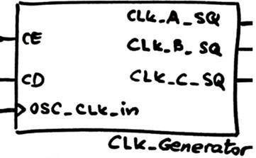
Fig. 8. CLK generator symbol. |
Your instructor will assign you a set of frequencies:
Option #1: fMUX_CLK = 6.4 kHz (fW = 800 Hz); fS_CLK = 1.2 kHz; fSYS_CLK = 200 Hz
Option #2: fMUX_CLK = 12 kHz (fW = 1.5 kHz); fS_CLK = 1.8 kHz; fSYS_CLK = 175 Hz
Option #2: fMUX_CLK = 9.6 kHz (fW = 1.2 kHz); fS_CLK = 1.4 kHz; fSYS_CLK = 168 Hz
Project location:
C:\CSD\P8\dimmer\(files)
Synthesise the project verifying the total number of D_FF.
Draw a testbench fixture to check how to complete Dimmer dedicated processor works.
- Design step #4. Timer for a sound signal
(optional, only if you have spare time and the previous design steps work correctly).
Complete the circuit in Fig. 3 adding the Chip6: a Timer that generates a sound beep for 2 s when the maximum or minimum light intensity is reached. Modify the Chip1 FSM diagram if required.
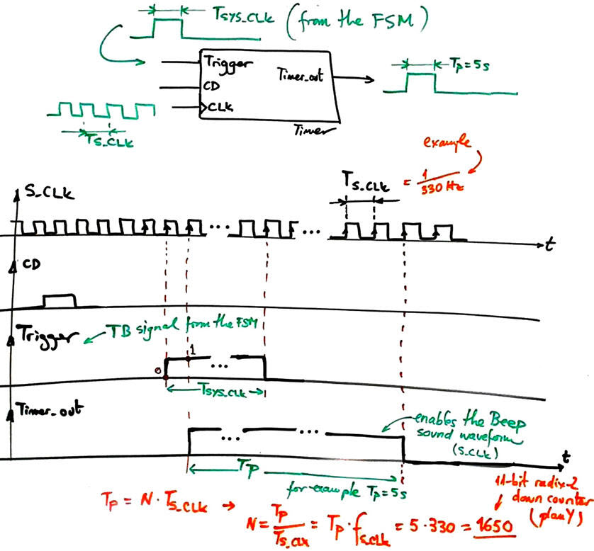
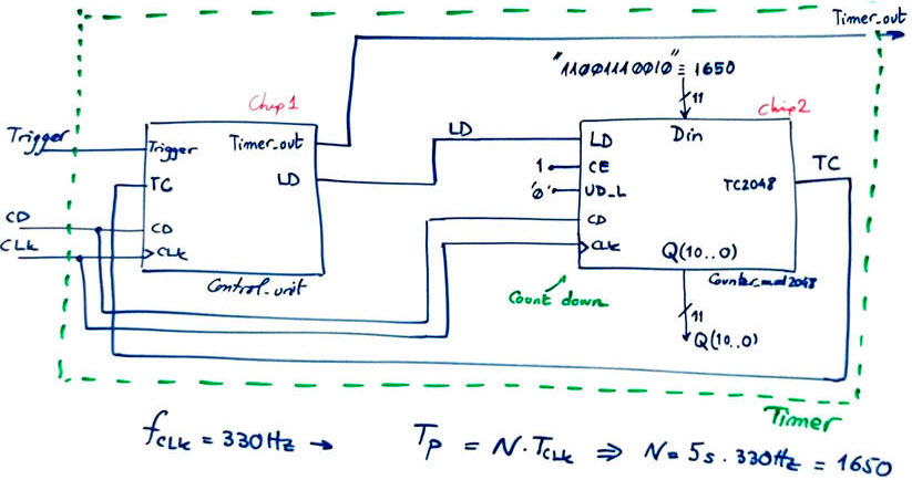
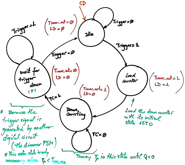
Fig. 9 is an example of a timer that you can adapt to your S_CLK option. For example, design a Timer for TP = 5 s from fS_CLK = 330 Hz. As its own datapath we use a down-counter Counter_mod2048 that counts N CLK periods when triggered.
   |
|
Fig. 9. Timer symbol and ideas for designing it. For this application, the additional state Wait_for_Trigger_down after having elapsed the timing period TP is not required; after Down_counting, the FSM can jump to Idle. For instance, using option #1 frequencies, the duration of the Trigger pulse is only TSYS_CLK = 5 ms. |
Project location:
C:\CSD\P8\dimmer\(files)
Design phase #2: ON/OFF switch
(optional, only if you have spare time and the design phase #1 works correctly).
We can implement an ON/OFF switch for the dimmer. When ON from whatever value of light intensity, if the user presses one of the two buttons more that 2 s, the light is turned off. Likewise, when OFF, pressing again more than 2 s any push button, turns on the light to the previously recorded light intensity.
Project location:
C:\CSD\P8\dimmer2\(files)
Design phase #3: Presence detector for saving energy.
(optional, only if you have spare time and the design phase #2 works correctly).
Modify the circuit adding a Timer and a presence or motion detector (PD), so that after 3.2 minutes of detecting no one in the room, the system goes to Off_state, as a way to save energy as in most modern buildings. Another interesting option is to disable the lamp on daylight when installed outdoors.
 |
|
Fig. 10. Commercial presence detector. |
Project location:
C:\CSD\P8\dimmer3\(files)
Design phase #4: IR remote control
(optional, only if you have spare time and the design phase #2 works correctly).
Add an infrared (IR) transmitter/receiver module to operate the lamp Dimmer using a remote control in the same way that we use the wall pushbuttons.
Project location:
C:\CSD\P8\dimmer4\(files)
Chapter 2 problems/h3> |
- D2.5 - |
LED lamp dimmer (FPGA-VHDL) |
V2 |
1. Specifications (Version #2)
Optional, advanced material. This alternative V2 full PWM control project is proposed at the DEE dimmer capstone project as the Option #B1 on using the DE10_Lite FPGA board to provide a digital control of the lamp. The idea is to implement in an FPGA the Microchip PWM module peripheral.
| Home Term 26/27-Q1 Contact Products Electronic devices and companies Software Books Magazines Instruments DEE Library EETAC DEEL |

|
|
| Web activa des de 09/2001, @ F. J. Robert, Web editat amb Microsoft Expression Web 4. El contingut és un complement als materials d'estudi del curs Circuits i Sistemes Digitals disponibles al campus digital Atenea. Llicència:Reconeixement 4.0 Internacional de Creative Commons |