|
|
Bachelor's Degree in Telecommunications Systems and in Network Engineering |
|
Chapter 2 problems |
- D2.1 - |
CD-MP3 player buttons controller (FPGA -VHDL) |
|
1. Specifications
Design phase #1: basic FSM
Our aim is to design a CD-MP3 player controller based on mechanical buttons and switches available on the front panel as pictured in Fig. 1. Other similar devices and applications have tactile screens or keypads.
The same project as an alternative design programming a μC is proposed in D3.1.
 |
| Fig. 1. CD-MP3 player application and its symbol. |
Buttons will be sampled at the system frequency fCLK indicated as an option in design phase #3. The pause LED L will be blinking when in pause. The output M is for running the motor to spin de compact disc and be able to read the audio files. When the CD is loaded and the door switch Op_L is closed, it generates a '0'. You can use inverter gates to generate active-high inputs Pp, Sp and Op to your system.
Draw an example of timing diagram to visualise the idea of the circuit.
 |
| Fig. 2. Example timing diagram. |
Find commercial devices where similar buttons control how the music is played (Hi-Fi audio chain, Bluetooth earbud, DVD player, etc.)
2. Planning ideas for the design phase #1
The planning is based on applying our FSM recipe in L6.1.(from section c to f). This architecture is translated to VHDL as a plan C1 single file where the three main components are translated as processes. We can propose a state diagram and do it in two steps to make it easier. For instance:
- Design step #1: Player with a single button Play/Pause (Pp).
It may operate like the wall push-button to turn ON and OFF the classroom luminaries (study the tutorial in LAB6). Clicking one time, the CD player motor starts spinning (M = '1'); clicking another time, it pauses (M = '0').
Project location: C:\CSD\P6\MP3_player1\(files)
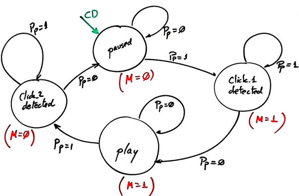 |
| Fig. 3. CD-MP3 player FSM state diagram for design step #1. |
Therefore, only when this step #1 is completely developed and tested (1-2-3-4), you can enhance the basic state diagram considering additional buttons and switches.
- Design step #2: Player with buttons Play/Pause (Pp) and Stop (Sp) and also with the loading door switch Open (Op).
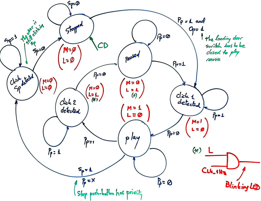 |
| Fig. 4. CD-MP3 player FSM state diagram proposed for the design step #2. When stopped, the only way to play music spinning the disc is with the loading door closed (Op = 1). The signal Sp has priority over Pp. Blinking the LED generating an intermittency is possible ANDing the output L with a low frequency squared digital waveform. We may imagine that the machine initial state is stopped, for the user can load and unload the disc. |
Project location:
C:\CSD\P6\MP3_player2\(files)
Adapt the FSM architecture to this problem, naming and connecting all signals and inputs and outputs.
Deduce how many D_FF are required when encoding FSM states using the following options and draw the state register memory:
Option #1: radix-2 (sequential)
Option #2: Gray
Option #3: Johnson
Option #4: one-hot
Draw the state register memory block.
Write the truth table of CC2 and CC1 and their equivalent behavioural interpretations (plan B) using flowcharts.
Write the FSM VHDL file.
Start a Quartus Prime synthesis project for one of the following programmable target chips:
Option #1: Cyclone IV EP4CE115F29C7
Option #1: MAX II EPM2210F324C3
Option #3: MAX 10 10M50DAF484C7 (*)
(*) Remember that this chip does not generate sdo delay files, thus use another one when gate-level simulations are required.
Inspect and annotate the RTL and technology views. Check the number of D_FF synthesised in this application.
Generate a VHDL testbench fixture schematic. Translate the timing diagram sketch from the specifications into de corresponding stimulus processes.
Run functional simulations to verify your design. Visualise as well in the wave timing diagram the internal states.
Run gate-level simulations to measure the propagation time CLK to output (tCO). Measure the minimum TCLK period or the maximum frequency of operation of the FSM.
Design phase #2: FSM + datapath
Generate a confirming user action beep (1.4 kHz audible sound wave for 0.9 s) every time the user clicks play/pause.
Enhance your device adding at least one of the following new features:
- To save battery, add operational resources to switch off the device when paused for 2 min.
- Indicate in seven-segment displays the time MM:SS the device is playing.
Project location: C:\CSD\P7\MP3_player\(files)
Each new specification will require additional circuits or extra states, basically for real-time counting. For example, as shown in Fig. 5, we can imagine modifying the state diagram to generate a clean synchronous pulse TB for triggering the 0.9 s timer after detecting the Pp click to play. The same for the detection of the pause click (generate a pulse TBp).
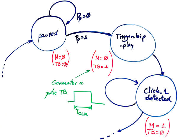 |
| Fig. 5. One CLK period state to generate a trigger pulse for the timer. |
During this timing period TP = 0.9 s, the 1.4 kHz square signal will be gated to the speaker.
Design phase #3: CLK_Generator
Design the CLK generator circuit from a 50 MHz quartz crystal oscillator to obtain all the clocking signals required to drive the application. Deduce the number of D_FF that the full project MP3_player will require.
Project location: C:\CSD\P8\MP3_player\(files)
The options for the system CLK are:
Option #1: fCLK = 330 Hz
Option #2: fCLK = 220 Hz
Option #3: fCLK = 150 Hz
An initial internal schematic to discuss the resources that may be required for completing phase #2 and phase #3 is represented in Fig. 6 (modify it as necessary).
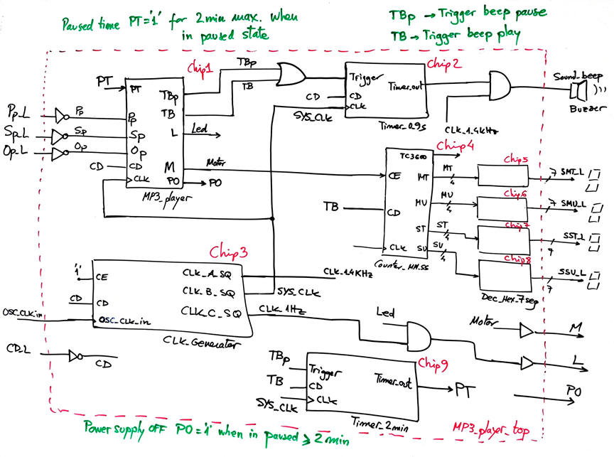 |
| Fig. 6. The idea of the MP3_player_top. The real-time counter is enabled while the motor is spinning (M = '1'). The beep is generate for both, detecting the play and also the pause clicks. The TBp will clear it. |
You can adapt the timers from this D2.21 version A.
The We can switch off the power supply to disconnect the circuit from the battery using Chip9 timer output paused time (PT). This signal will be high if the player is less than 2 min. in paused state.
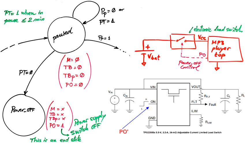 |
| Fig. 7. The idea of switching off the application and save energy. If at paused state and TP = '0', it means that the system has remained in it for 2 min. A power off (PO) control output can drive an electronic power switch to disconnect the load MP3_player_top. These a two examples of such devices: TI TPS22950, Torex XC6193. |
| Home Term 26/27-Q1 Contact Products Electronic devices and companies Software Books Magazines Instruments DEE Library EETAC DEEL |

|
|
| Web activa des de 09/2001, @ F. J. Robert, Web editat amb Microsoft Expression Web 4. El contingut és un complement als materials d'estudi del curs Circuits i Sistemes Digitals disponibles al campus digital Atenea. Llicència:Reconeixement 4.0 Internacional de Creative Commons |