

|
Bachelor's Degree in Telecommunications Systems and Network Engineering |

|
Chapter 2 problems |
- B3.7 - |
Multiplexed displays: A: 7-segment |
B: LED bar |
1. Specifications
Because microcontrollers typically have a limited number of pins, implementing a multiplexed display system (MDS) is an effective way to reduce the required pin count when multiple displays are needed. Review the MDS tutorial for more details. For instance, a 10-digit calculator display requires only 17 pins to display any number from 0000000000 to 9999999999, with the Binary-Coded Decimal (BCD) data stored in 10 bytes of RAM.
The same project is proposed in D1.7 as a combinational circuit based on logic gates.
We can design the BCD_7seg_MUX_3digit represented in Fig. 1. To practise with polling inputs, we will imagine that the H, T and U data is external, generated by 12 switches. Select signal S(1..0) can be generated externally for example at 1 kHz by a modulo 3 counter, S = 0, 1, 2, 0, 1, 2, 0, ... and will multiplex the numbers to the corresponding displays.
- When S = 0, CA_L = "110" and the number U is decoded at segment outputs to be represented on digit 0.
- When S = 1, CA_L = "101" and the number T is decoded at segment outputs to be represented on digit 1.
- When S = 2, CA_L = "011" and the number H is decoded at segment outputs to be represented on digit 2.
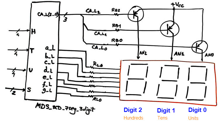 |
Fig. 1. Symbol for this MDS_HEX_7seg_3digit and the external driving circuit for the common anodes. Only one digit is activated at a time. |
A) Planning hardware
Pin assignment option #1:
| H(3..2) ---> RD(7..6) | H(1..0) ---> RC(1..0) | |
| T(3..2) ---> RD(5..4) | T(1..0) ---> RC(3..2) | |
| U(3..2) ---> RD(3..2) | U(1..0) ---> RC(5..4) | |
| S(1..0) ---> RD(1..0) | ||
| CA_L(2..0) ---> RB(7..5) | ||
| a_L, b_L, c_L, d_L ---> RB(4..1) | e_L, f_L, g_L ---> RA(3..1) |
Pin assignment option #2:
| H(3..2) ---> RA(5..4) | H(1..0) ---> RB(7..6) | |
| T(3..2) ---> RB(5..4) | T(1..0) ---> RD(7..6) | |
| U(3..1) ---> RD(5..3) | U(0) ---> RC(7) | |
| S(1..0) ---> RC(6..5) | ||
| CA_L(2..0) ---> RC(4..2) | ||
| a_L, b_L ---> RC(1..0) | c_L, d_L, e_L, f_L ---> RA(3..0) | g_L ---> RB(2) |
Pin assignment option #3:
| H(3..1) ---> RC(7..5) | H(0) ---> RD(7) | |
| T(3..0) ---> RD(6..3) | ||
| U(3..2) ---> RB(7..6) | U(1..0) ---> RA(5..4) | |
| S(1..0) ---> RA(3..2) | ||
| CA_L(2..0) ---> RB(5..3) | ||
| a_L, b_L, c_L ---> RD(2..0) | d_L, e_L, f_L, g_L ---> RC(4..1) |
Project location:
C:\CSD\P9\MDS_BCD_7seg_3digit\(files)
Chapter 2 problems |
- B3.7 - |
Multiplexed displays: A: 7-segment |
B: LED bar |
1. Specifications
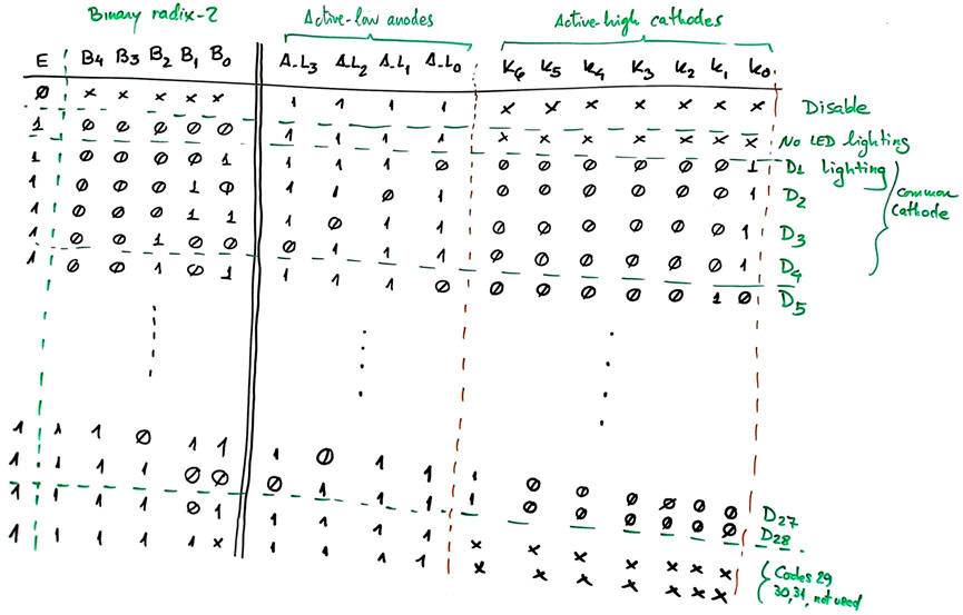
In this project we propose to use a µC PIC18F48K22 to implement the combinational circuit Bar_28LED_dec represented in Fig. 1. The same project is proposed in D1.7 as a combinational circuit based on logic gates (complete and use the truth table in Fig. 7).
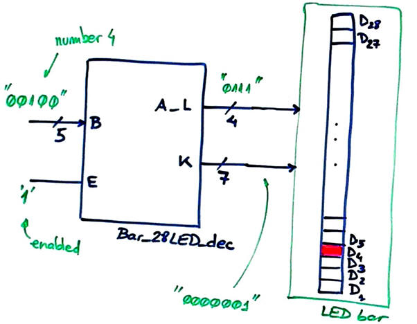 |
Fig. 1. Symbol of the Bar_28LED_dec. |
A) Planning hardware
To practise with polling inputs we will imagine a hardware circuit in Proteus where number B and enable E are generated by 6 switches. You can also use the schematic "Hex_7seg_MUX_2digit.pdsprj" to drive le LED bar and check results.
Copy and adapt a circuit from any of the previous projects (LAB9) and name it "Bar_28LED_dec.pdsprj". Assign pins to inputs and outputs accordingly to one of the following options (your instructor will tell you which):
Pin assignment option #1:
| B(4..3) ---> RD(7..6) | B(2..0) ---> RC(5..3) | |
| E ---> RE(1) | ||
| A_L(3..2) ---> RB(7..6) | A_L(1..0) ---> RC(7..6) | |
| K(6..5) ---> RA(3..2) | K(4..3) ---> RB(4..3) | K(2..0) ---> RD(3..1) |
Pin assignment option #2:
| B(4..3) ---> RC(5..4) | B(2..0) ---> RD(7..5) | |
| E ---> RB(1) | ||
| A_L(3..2) ---> RA(3..2) | A_L(1..0) ---> RB(6..5) | |
| K(6..5) ---> RC(7..6) | K(4..3) ---> RD(4..3) | K(2..0) ---> RE(2..0) |
Pin assignment option #3:
| B(4..3) ---> RE(2..1) | B(2..0) ---> RA(3..1) | |
| E ---> RD(7) | ||
| A_L(3..2) ---> RB(1..0) | A_L(1..0) ---> RC(7..6) | |
| K(6..5) ---> RB(5..4) | K(4..3) ---> RC(1..0) | K(2..0) ---> RD(5..3) |
Project location:
C:\CSD\P9\Bar_LED28_dec\(files)
B) Planning software
Organise the main program in our CSD way.
Propose a hardware-software diagram naming all the electrical signals, RAM variables and the software functions.
Explain how to configure the µC in init_system(). List all RAM variables required and their type.
Organise using a flowchart the interface function read_inputs().
Organise using a flowchart the interface function write_outputs().
Infer the truth_table() software function using a behavioural interpretation and the corresponding flowchart.
Developing & testing (debugging)
Write the "Bar_28LED_dec.c" source code translating the function flowcharts. Start capturing only one input as in (LAB9) and visualising it in the watch window. And only then go step by step developing & testing more inputs.
Start a software IDE project for the target microcontroller PIC18F46K22 and generate the configuration files ".cof" and ".hex" after compilation. Discuss the project summary: % of ROM used for the code, number of RAM bytes used, etc.
Add a few lines of code every time, compile and run the test interactively to check results watching variables.
| Note: Step-by-step tactical approach for developing and testing the project: Read one input at a time and run to check that the voltage value is correctly captured as a valid digital value in RAM memory. Write one output at a time and run to check that your code is correct to light the LED connected at the output pin. |
Measure how long does it take to run the main loop code when using a 4 MHz and a 20 MHz crystal oscillators.
NOTE (optional): This project can be continued using the software implementation of FSM proposed in P10 to complete the the full Bar_28LED.
| Home Term 26/27-Q1 Contact Products Electronic devices and companies Software Books Magazines Instruments DEE Library EETAC DEEL |

|

|
| Web activa des de 09/2001, @ F. J. Robert, Web editat amb Microsoft Expression Web 4. El contingut és un complement als materials d'estudi del curs Circuits i Sistemes Digitals disponibles al campus digital Atenea. Llicència:Reconeixement 4.0 Internacional de Creative Commons |