

|
Bachelor's Degree in Telecommunications Systems and Network Engineering |

|
Chapter 1 problems |
- D1.6 - |
20-sensor water tank level meter with 7-segment reading |
1.- Specifications
Design the circuit Tank_20level_meter represented in Fig. 1 studying and adapting ideas from the L2.5 lecture on incomplete truth tables.
The same project B3.6 is proposed in Chapter 3 for learning the basics of μC software organisation and basic digital I/O.
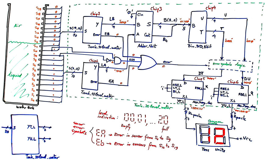 |
|
Fig.1. The tank level meter idea built using digital optical sensors (1), (2) attached to the tank wall. |

Draw an example of timing diagram to be used later as stimulus in the VHDL testbench when verifying the synthesised circuit. Consider Min_Pulse = 5.21 ms.
CPLD or FPGA target chip options:
option #1.: MAX II
option #2.: MAX 10 (*)
option #3.: Cyclone IV
(*) MAX10 chips are not used for running gate-level ModelSim simulation because Intel Quartus Prime does not generate the "*.sdo" file accompanying the "*.vho" translation of the technology view. Thus, you can run the timing analyser as usual, and change to another device family for performing examples of gate-level timing diagrams.
How many FPGA resources (logic cells, logic elements, etc.) are used? What is the percentage of the target chip used in this design?
2. Planning
Plan A: Structural circuit based on logic gates and equations in a single VHDL file. We have many strategies, for instance:
Design the Chip1 Tank_10level_meter.
option #1: use Minilog to obtain PoS.
Project location:
C:\CSD\P2\Tank_10level_meter_PoS\(files)
Be aware to report these items.
How many FPGA resources (logic cells, logic elements, etc.) are used? What is the percentage of the target chip used in this design?
option #2: use Minilog to obtain SoP.
Project location:
C:\CSD\P2\Tank_10level_meter_SoP\(files)
Be aware to report these items.
How many FPGA resources (logic cells, logic elements, etc.) are used? What is the percentage of the target chip used in this design?
Plan B: Behavioural approach writing the truth table or the high-level description or algorithm in VHDL in a single file (flat).
Design the Chip1 Tank_10level_meter.
Project location:
C:\CSD\P2\Tank_10level_meter_B\(files)
Be aware to report these items.
How many FPGA resources (logic cells, logic elements, etc.) are used? What is the percentage of the target chip used in this design?
Plan C2 is a hierarchical architecture based (multiple VHDL file) on components and signals. For instance, let us it to solve the complete Tank_20level_meter proposed in Fig. 1 consisting of several chips and logic. Find and adapt components from our tutorials.
C:\CSD\P3\Tank_20level_meter\(files)
Be aware to report these items.
How many FPGA resources (logic cells, logic elements, etc.) are used? What is the percentage of the target chip used in this design?
How many VHDL files contains this project?
After having studied P4 tutorials, additional questions can be added to our report. For instance:
-
Perform a gate-level simulation to measure propagation delays in a given signal transition.
-
Deduce the worst-case propagation delay running the timing analyser tool and calculate the circuit's maximum frequency of operation for the target chip used in the design.
| Home Term 26/27-Q1 Contact Products Electronic devices and companies Software Books Magazines Instruments DEE Library EETAC DEEL |

|

|
| Web activa des de 09/2001, @ F. J. Robert, Web editat amb Microsoft Expression Web 4. El contingut és un complement als materials d'estudi del curs Circuits i Sistemes Digitals disponibles al campus digital Atenea. Llicència:Reconeixement 4.0 Internacional de Creative Commons |