

|
Bachelor's Degree in Telecommunications Systems and Network Engineering |

|
Chapter 1 problems |
- D1.5 - |
Encoders. A: PBX door phone B: 32-key gamer keypad |
1. Specifications
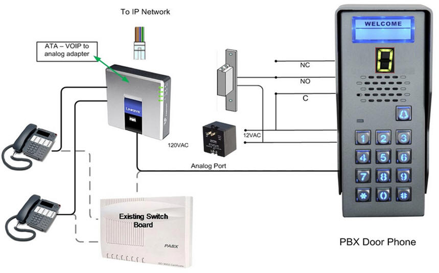
The project objective is to design an encoder Enc_12_4 similar to the one presented in the tutorial Enc_10_4 using VHDL synthesis and verification tools. For instance, the application can be integrated as a subsystem in a professional PBX door phone with dialing keypad as represented in Fig. 1. The device has to generate the 4-bit binary code of the clicked key. BCD codes for keys from 0 to 9, "1010" for the hash symbol "#" and "1011" symbol for the asterisk symbol "*". Group select output GS has to be held high while any key is pressed. The encoder also has enable input Ei and enable output Eo to detect when it is disabled and when is active but no one is pressing keys. Use a 7-segment decoder from any of the tutorials to represent the code of the key pressed.
The same project B3.5 is proposed in Chapter 3 for learning the basics of μC software organisation and basic digital I/O.
 |
|
Fig. 1. The keyboard that has to be interfaced to a commercial private branch exchange (PBX) phone and the commercial reference of the diagram. |
Propose the symbol and truth table of this Enc_12_4 adapting other encoder examples.
Draw an example of timing diagram to be used later as stimulus in the testbench when verifying the synthesised circuit. Consider Min_Pulse = 2.67 ms.
As a good design strategy, you can organise the project in two design phases:
- phase #1: You can imagine a symbol and a circuit similar to the Enc_10_4 and so not including yet the outputs a, b, c, d, e, f, and g to be able to connect a 7-segment display. Develop and test this project. When this circuit with only binary radix-2 outputs Y(3..0) works correctly, and only if you have more time,
- phase #2: Add the new segment outputs to the phase #1 truth table so that you can also light a 7-segment display as shown in Fig.1.
CPLD or FPGA target chip options:
option #1.: MAX II
option #2.: MAX 10 (*)
option #3.: Cyclone IV
(*) MAX10 chips are not used for running gate-level ModelSim simulation because Intel Quartus Prime does not generate the "*.sdo" file accompanying the "*.vho" translation of the technology view. Thus, you can run the timing analyser as usual, and change to another device family for performing examples of gate-level timing diagrams.
How many FPGA resources (logic cells, logic elements, etc.) are used? What is the percentage of the target chip used in this design?
2. Planning
Plan A: Find equations and write them in a single VHDL file. For example:
option #1: PoS from Minilog minimisation software or by inspection of the truth table. Write down the single-file (flat) VHDL code using equations. Synthesise and test.
Project location:
C:\CSD\P2\Enc_12_4_PoS\(files)
option #2: SoP from Minilog minimisation software or by inspection of the truth table. Write down the single-file (flat) VHDL code using equations. Synthesise and test.
Project location:
C:\CSD\P2\Enc_12_4_SoP\(files)
Be aware to report these items.
Plan B: capture in a single VHDL file the truth table drawing firstly an schematic. Synthesise and test.
Project location:
C:\CSD\P2\Enc_12_4_B\(files)
Be aware to report these items.
Plan C2: Draw a hierarchical circuit using Enc_4_2 components and logic gates if necessary. Synthesise and test.
Project location:
C:\CSD\P3\Enc_12_4_C2\(files)
Be aware to report these items.
Chapter 1 problems |
- D1.5 - |
Encoders. A: 12-to-4 B: 30-key gamer keypad |
1. Specifications
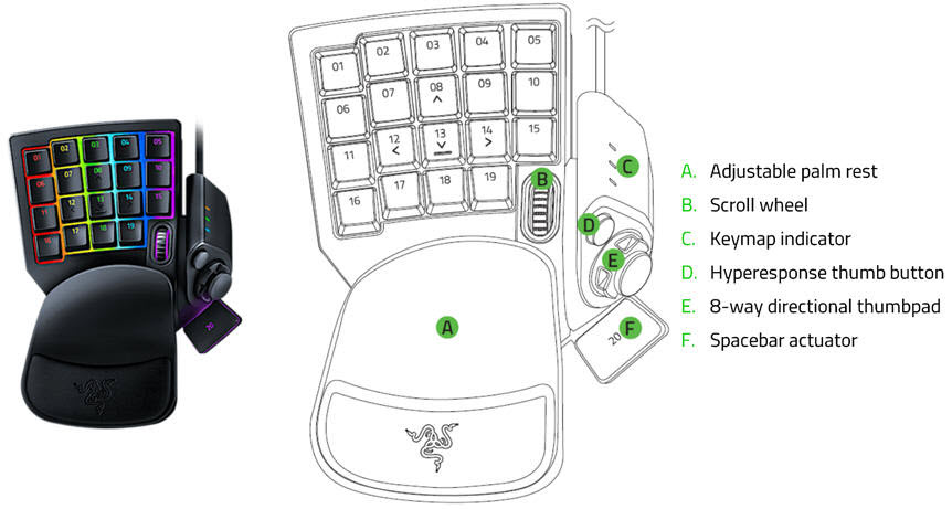
We want to design the encoding section of the commercial product from Razer represented in Fig. 1. It is not a complete keyboard, it cannot be used for typing or as a full keyboard replacement. It is designed specifically for gaming controls.
As shown in the user manual, the peripheral has 19 standard keys numbered from 1 to 19 and other push-buttons or switching actuators. Generate a 5-bit binary code for each pressed key with priority high accordingly to this table:
Key |
Output binary code |
Decimal number |
| F: spacer actuator | "00000" | 0 |
| Key 01, 02, 03, …, 19 | "00001", "00010", "00011", …, "10011" | 1, 2, 3, ..., 19 |
| D: hyper response thumb button | "10100" | 20 |
| C: Scroll wheel up | "10101" | 21 |
| C: Scroll wheel down | "10110" | 22 |
| C: Scroll wheel click | "10111" | 23 |
| E: 8-way directional thumb pad | "11000", "11001", …, "11111" | 24, 25, 26, ..., 31 |
 |
|
Fig. 1. Picture of the 32-key keypad Razer Tartarus Pro. |
Use priority high to output the code with the highest value when several keys or buttons are pressed simultaneously.
Draw an example of timing diagram to be used later as stimulus in the VHDL testbench when verifying the synthesised circuit. Consider Min_Pulse = 3.67 µs.
CPLD or FPGA target chip options:
option #1.: MAX II
option #2.: MAX 10 (*)
option #3.: Cyclone IV
(*) MAX10 chips are not used for running gate-level ModelSim simulation because Intel Quartus Prime does not generate the "*.sdo" file accompanying the "*.vho" translation of the technology view. Thus, you can run the timing analyser as usual, and change to another device family for performing examples of gate-level timing diagrams.
How many FPGA resources (logic cells, logic elements, etc.) are used? What is the percentage of the target chip used in this design?
2. Planning
We have two planning strategies for such a circuit: (1) matrix scanning as shown in the highlighted project P6, and combinational logic cascading smaller components of the same kind and logic gates when necessary. This second options is chosen in this application to learn the basics of plan C2 for writing schematics in VHDL.
Plan A: Design an Enc_8_3 structural circuit type 74LS148 based on logic gates and equations in a single VHDL file. We have many strategies, for instance:
option #1: use Minilog to obtain PoS.
In the tutorial Enc_10_4 you have an example to study, copy and adapt.
Project location:
C:\CSD\P2\Enc_8_3_PoS \(files)
How many FPGA resources (logic cells, logic elements, etc.) are used? What is the percentage of the target chip used in this design?
 |
Fig. 2. Enc_8_3 symbol. |
option #2: use Minilog to obtain SoP for the same symbol in Fig. 2.
In the tutorial Enc_10_4 you have an example to study, copy and adapt.
Project location:
C:\CSD\P2\Enc_8_3_SoP \(files)
Be aware to report these items.
In the highlighted project P2 you have an example of an HEX to 7-segment decoder.
How many FPGA resources (logic cells, logic elements, etc.) are used? What is the percentage of the target chip used in this design?
Plan B: Design a Enc_16_4 drawing a high-level algorithm description (flowchart) or schematic to the translated into VHDL in a single file (flat).
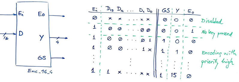 |
Fig. 3. Enc_16_4 symbol. |
In the tutorial Enc_10_4 you have an example to study, copy and adapt.
Project location:
C:\CSD\P2\Enc_16_4_B\(files)
Be aware to report these items.
How many FPGA resources (logic cells, logic elements, etc.) are used? What is the percentage of the target chip used in this design?
Plan C2: Design and test the top Enc_32_5 architecture using smaller components of the same kind, logic gates and other combinational circuits when necessary.
option #1: Use Enc_16_4 components and the circuit expansion technique proposed in datasheets.
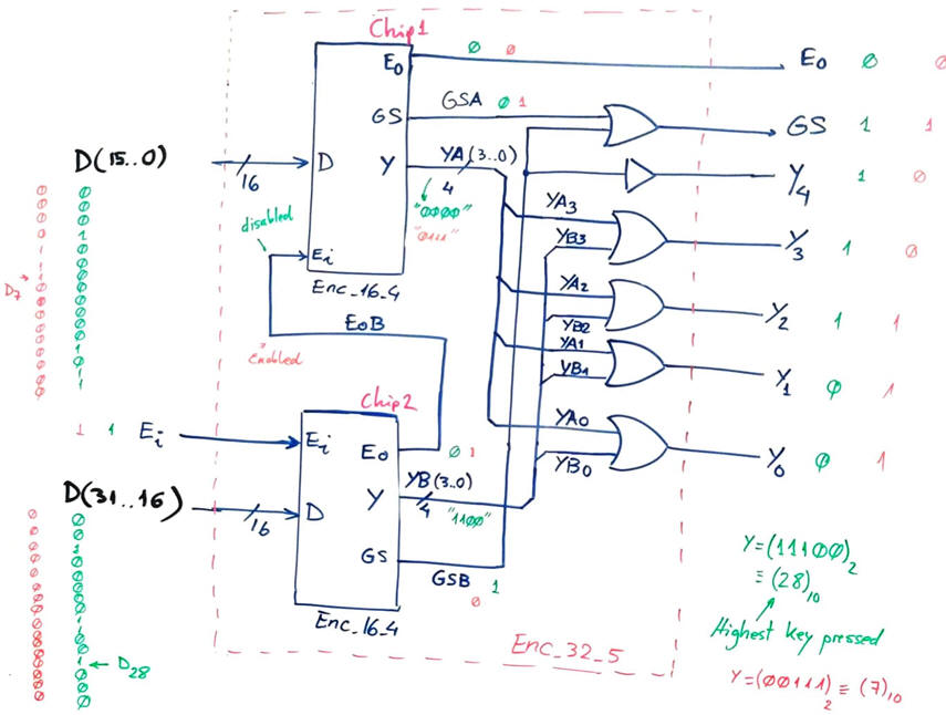 |
Fig. 4. Enc_32_5 proposed schematic copied and adapted from the 74LS148 datasheet. Two input vectors are tested, shown in green and orange. |
In the tutorial Enc_10_4 you have an example to study, copy and adapt.
Project location:
C:\CSD\P3\Enc_32_5E\(files)
Be aware to report these items.
How many FPGA resources (logic cells, logic elements, etc.) are used? What is the percentage of the target chip used in this design?
How many VHDL files contains this project?
option #2: Use Enc_8_3 components in a tree structure proposed by AI or found in books.
For instance, prompt "Design a schematic for an encoder 32-to-5 using a tree of encoders 8-to-3" in Claude.ai or Mistral Vibe to obtain diagrams as shown in Fig. 5, which is similar to what you can find in books. These materials are ready for group discussion.
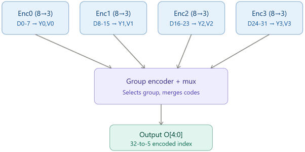 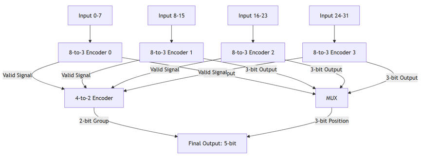 |
Fig. 5. Diagrams on the design of the Enc_32_5 generated by Claude.ai and Mistral Vibe. |
NOTE on the use of AI tools: To make it systematic, simple, easy to learn and explain, and also easy to correct, in CSD we do not copy and develop final results from AI tools, but translate ideas or algorithms like these examples in Fig. 5 into fully annotated electronic schematics ready for translation into VHDL, as shown in Fig. 6.
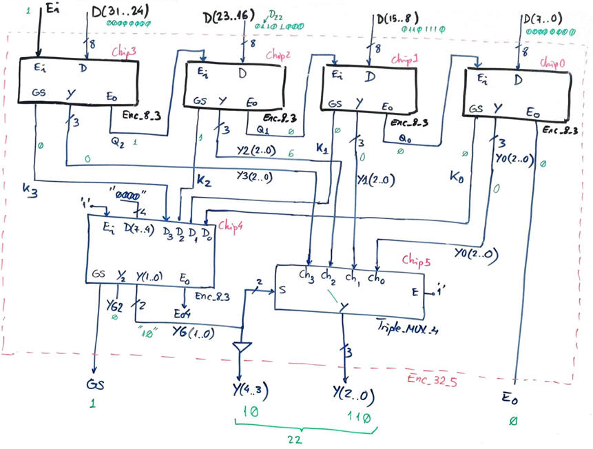 |
Fig. 6. Proposed schematic in a tree structure elaborated from the sketches in Fig. 5 to be used in CSD. An input test vector is depicted in green; add other test inputs in your ModelSim testbench. |
In the tutorial Enc_10_4 you have an example to study, copy and adapt.
Project location:
C:\CSD\P3\Enc_32_5T\(files)
Be aware to report these items.
How many FPGA resources (logic cells, logic elements, etc.) are used? What is the percentage of the target chip used in this design?
How many VHDL files contains this project?
After having studied P4 tutorials, additional questions can be added to our report. For instance:
-
Perform a gate-level simulation to measure propagation delays in a given signal transition.
-
Deduce the worst-case propagation delay running the timing analyser tool and calculate the circuit's maximum frequency of operation for the target chip used in the design.
| Home Term 26/27-Q1 Contact Products Electronic devices and companies Software Books Magazines Instruments DEE Library EETAC DEEL |

|

|
| Web activa des de 09/2001, @ F. J. Robert, Web editat amb Microsoft Expression Web 4. El contingut és un complement als materials d'estudi del curs Circuits i Sistemes Digitals disponibles al campus digital Atenea. Llicència:Reconeixement 4.0 Internacional de Creative Commons |