|
|
Bachelor's Degree in Telecommunications Systems and in Network Engineering |
|
|
|
|||||
Chapter 1 problems |
- D1.4 - |
Designing Circuit_VT using plan A, plan B, and plan C2 |
|||
|
|
|||||
1. Specifications
Designing combinational circuits from P1.
Option #1: Design the combinational Circuit_VT in Fig. 1 in a programmable logic device (PLD) target chip using one of the following plans and VHDL EDA tools (design flow). The synthesised circuit will be tested using VHDL testbenches.
The same project B3.4 is proposed in Chapter 3 for learning the basics of μC software organisation and basic digital I/O.
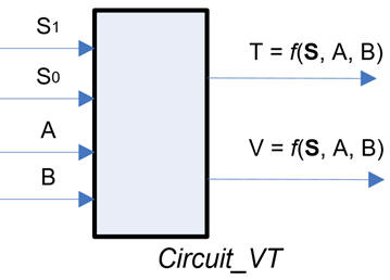 |
Fig. 1. Symbol and truth table of the circuit to be designed. Be aware that in this symbol, inputs S(1..0) are represented in multi-wire vector form. |
Draw an example of timing diagram to be used later as stimulus in the VHDL testbench when verifying the synthesised circuit. Consider Min_Pulse = 1.45 ms.
CPLD or FPGA target chip options:
Target #1.: MAX II
Target chip #2.: MAX 10
Target chip #3.: Cyclone IV
2. Planning
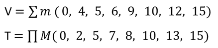
Plan A structural circuit based on logic gates considering these options:
option #1: Output V contains only-NAND from the canonical sum of minterms. Output T using only 2-input NOR (NOR2) from the minimised PoS equation from minilog.
Project location:
C:\CSD\P2\Circuit_VT\planA1\(files)
 |
|
Fig. 2. Planning the Circuit_VT using logic gates (visio). |
option #2: Output V contains only-NOR from the canonical product of maxterms. Output T using only 2-input NAND (NAND2) from the minimised SoP equation from minilog.
Project location:
C:\CSD\P2\Circuit_VT\planA2\(files)
Plan B behavioural approach writing the truth table in VHDL.
Project location:
C:\CSD\P2\Circuit_VT\planB\(files)
Plan C2 using the method of decoders (MoD).
Project location:
C:\CSD\P2\Circuit_VT\MoD\(files)
Plan C2 using the method of multiplexers (MoM) and a MUX_4 for T and a MUX_8 for V.
Project location:
C:\CSD\P2\Circuit_VT\MoM\(files)
Option #2: Design several versions of the combinational Circuit_G analysed in A1.6.
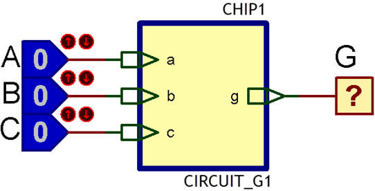
Plan A. Design an equivalent circuit for Circuit_G from its truth table, for example naming it Circuit_G1, minimising using minilog and using only NOR2.
|
|
Fig. 2. Combinational circuit g = f(a, b, c). |
Test the circuit using one of these analysis methods:
-
method II on Proteus. The laboratory prototype will contain only 74LS00 and 74LS02 chips.
-
method III on VHDL.
-
method IV on WolframAlpha.
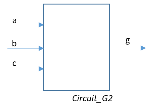
Plan B. Design an equivalent circuit for Circuit_G from its truth table, for example naming it Circuit_G2, capturing the truth table behaviour as an schematic or as a flowchart.
|
|
Fig. 3. Combinational circuit. g = f(a, b, c) |
Synthesise the circuit in VHDL by means of a Quartus Prime project for an FPGA target chip and verify it simulating a ModelSim testbench.
Plan C2 using the method of decoders (MoD).
Plan C2 using the method of multiplexers (MoM) and a MUX_8.
Option #3: Design several versions of the combinational Circuit_U analysed in A1.2
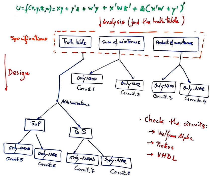
Plan A using only two-input NOR (NOR2) or only two-input NAND (NAND2). The representation in Fig. 1 is a map that can help to comprehend the concepts. From the circuit's truth table you can produce several circuits based on only-NAND or only-NOR gates.
 |
|
Fig. 1. Concept map to explain the idea of extracting several circuits from the same initial specifications. |
Test the circuit using one of these opcions:
- analysis method II on Proteus. The laboratory prototype will contain only 74LS00 or 74LS02 chips.
- analysis method III on VHDL.
- analysis method IV on WolframAlpha.
Write your report as usual following indications from our rubric.
Plan B behavoural approach writting the truth table in VHDL. To verify that your RTL works correctly, use ModelSim functional simulation.
Plan C2 using the method of decoders (MoD).
Plan C2 using the method of multiplexers (MoM) and a MUX_2.
| Home Term 24/25-Q1 Contact Products Electronic devices and companies Software Books Magazines Instruments DEE Library EETAC DEEL |

|
|
| Web activa des de 09/2001, @ F. J. Robert, J. Jordana. Web editat amb Microsoft Expression Web 4. El contingut és un complement als materials d'estudi del curs Circuits i Sistemes Digitals disponibles al campus digital Atenea. Llicència:Reconeixement 4.0 Internacional de Creative Commons |