|
|
Bachelor's Degree in Telecommunications Systems and in Network Engineering |
|
|
|
|||||
Chapter 1 problems |
- D1.3 - |
5-bit ones counter |
|||
|
|
|||||
1. Specifications
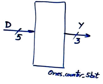
Design the 5-bit ones counter chip represented in Fig. 1 using a flat single VHDL file design (plan A or plan B) and following our VHDL design flow from L2.1.
The same project B3.3 is proposed in Chapter 3 for learning the basics of μC software organisation and basic digital I/O.
|
|
|
Fig.1. Ones_counter_5bit symbol. |
On the initial discussion of the project specifications:
To study how to draw the circuit truth table, you can explore tutorial projects Ones_counter_8bit and Ones_counter_4bit.
Draw an example of timing diagram to be used later as stimulus in the VHDL testbench when verifying the synthesised circuit. Consider Min_Pulse = 103.34 ns. How long does it take to complete all the circuit tests?
Discusss the several plans that we have available for designing combinational circuits.
Discuss our VHDL design flow. What are its main sections? What tools and instruments are involved? Why are we replacing schematic entries with VHDL descriptions?
CPLD or FPGA target chip options:
Target option #1.: MAX II
Target option #2.: MAX 10
Target option #3.: Cyclone IV
Discusss what is a field programmable gate array (FPGA) or a programmable logic device (PLD) target chip. What is its capacity? Discuss the schematic of one FPGA logic element.
2. Planning
Plan A structural circuit based on logic gates and equations in a single VHDL file. We have many estrategies, for instance:
option #1: use minilog to obtain PoS.
Project location:
C:\CSD\P2\Ones_counter_5bit_PoS\(files)
How many FPGA resources (logic cells, logic elements, etc.) are used? What is the percentage of the target chip used in this design?
option #2: use minilog to obtain SoP.
Project location:
C:\CSD\P2\Ones_counter_5bit_SoP\(files)
How many FPGA resources (logic cells, logic elements, etc.) are used? What is the percentage of the target chip used in this design?
Plan B behavioural approach writing the truth table or the high-level description or algorithm in VHDL in a single file (flat).
Project location:
C:\CSD\P2\Ones_counter_5bit_B\(files)
How many FPGA resources (logic cells, logic elements, etc.) are used? What is the percentage of the target chip used in this design?
| Home Term 24/25-Q1 Contact Products Electronic devices and companies Software Books Magazines Instruments DEE Library EETAC DEEL |

|
|
| Web activa des de 09/2001, @ F. J. Robert, J. Jordana. Web editat amb Microsoft Expression Web 4. El contingut és un complement als materials d'estudi del curs Circuits i Sistemes Digitals disponibles al campus digital Atenea. Llicència:Reconeixement 4.0 Internacional de Creative Commons |