|
|
Bachelor's Degree in Telecommunications Systems and in Network Engineering |
|
|
|
|||||
Chapter 1 problems |
- A1.6 - |
Analysing Circuit_G |
|||
|
|
|||||
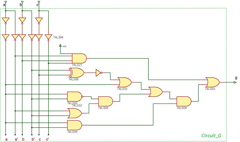
Using our analysis method I in CSD (L1.3) (Boolean algebra) find the circuit's symbol and truth table of the algebraic expression represented in Fig. 1. Name it as Circuit_G. Express the output as a sum of minterms and as a product of maxterms.
|
|
| Fig. 1. Combinational circuit g = f(a, b, c). |
Deduce the circuit algebraic equation.
Transform the algebraic expression to SoP (or PoS) using Boole algebra.
Transform SoP (or PoS) to a sum of minterms (or a product of maxterms). Draw the truth table.
Draw a timing diagram considering all binary combinations and constant Min_Pulse = 2.3 μs.
Project location to save your paper solution, class notes, pictures, theory, etc.:
C:\CSD\P1\Circuit_G\algebra\(files)
Verify your results solving the same project using another analysis method.
Using our analysis method II (Proteus, electronic circuit simulations) find the circuit's symbol and truth table of the algebraic expression represented in Fig. 1. Project locations to save the complementary project for checking results:
C:\CSD\P1\Circuit_G\proteus\(files)
Proteus components library options:
option #1.: LS-TTL
option #2.: CMOS
Verify your results solving the same project using another analysis method.
Using our analysis method III (VHDL EDA synthesis and simulation tools) find the circuit's symbol and truth table of the algebraic expression represented in Fig. 1. Project locations to save the complementary project for checking results:
C:\CSD\P1\Circuit_G\VHDL\(files)
Target chip options:
option #1.: MAX II
option #2.: MAX 10
option #3.: Cyclone IV
Verify your results solving the same project using another analysis method.
Using our analysis method IV (WolframAlpha, computer numerical engine) find the circuit's symbol and truth table of the algebraic expression represented in Fig. 1. Project locations to save the complementary project for checking results:
C:\CSD\P1\Circuit_G\wolfram\(files)
Verify your results solving the same project using another analysis method.
| Home Term 24/25-Q1 Contact Products Electronic devices and companies Software Books Magazines Instruments DEE Library EETAC DEEL |

|
|
| Web activa des de 09/2001, @ F. J. Robert, J. Jordana. Web editat amb Microsoft Expression Web 4. El contingut és un complement als materials d'estudi del curs Circuits i Sistemes Digitals disponibles al campus digital Atenea. Llicència:Reconeixement 4.0 Internacional de Creative Commons |