|
|
Bachelor's Degree in Telecommunications Systems and in Network Engineering |
|
|
|
||
|
|
Ones_counter_4bit plan C2: hierarchical multiple-file VHDL |
|
|
|
||
4-bit ones counter using the MoD
1. Specifications
Design a circuit to count the number of ones in its 4-bit input vector using a hierarchical approach plan C2 L3.3.
|
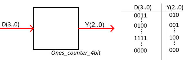
Fig. 1. Symbol and examples from the truth table of the 4-bit ones counter. [Visio] |
An alternative design using plan B of the ones_counter_4bit is presented in D1.3.
2. Planning
Invent the circuit architecture based on MoD. How many VHDL files will be required?
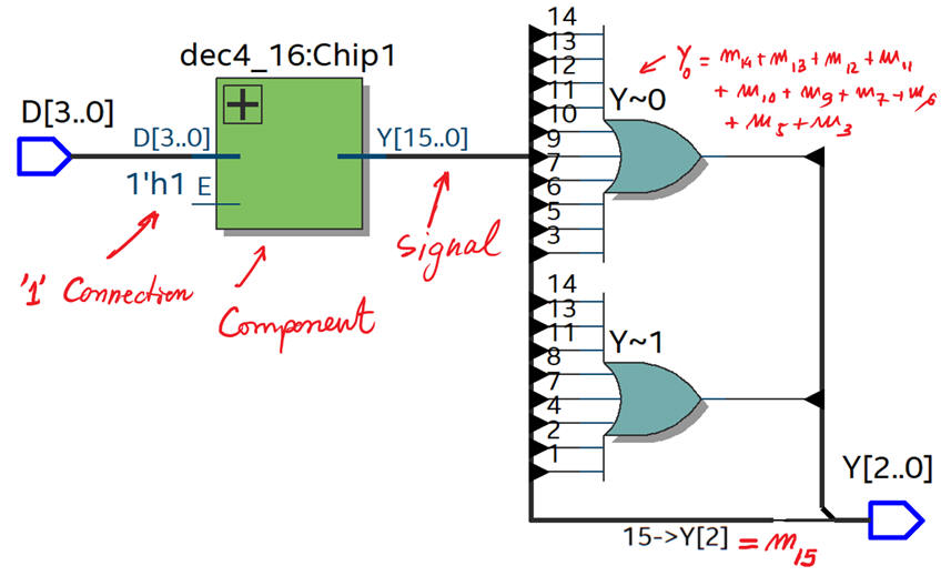
Writing down the full truth table, we infer the three output functions in canonical form, and thus the circuit in Fig. 2.
Y2 = m15
Y1 = m3 + m5 + m6 + m7 + m9 + m10 + m11 + m12 +m13 + m14
Y0= m1 + m2 + m4 + m7 + m8 + m11 + m13 + m14
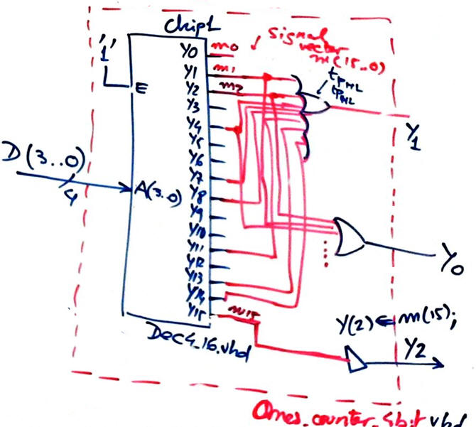 |
Fig. 2. Proposed architecture. |
Step #1.- Design the component Dec4_16 using any plan.
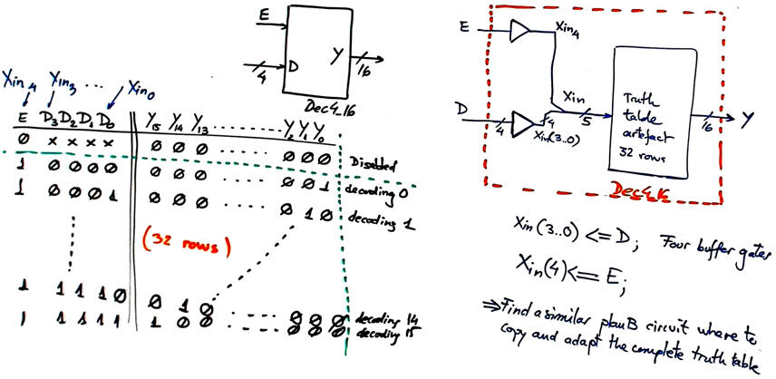 |
| Fig. 3. Plan B proposed for the Dec4_16. |
Step #2.- Design the top circuit in Fig. 2.
Project location:
C:\CSD\P3\Ones_counter_4bit_MoD\(files)
Target chip: Cyclone IV EP4CE115F29C7.
3. Developing the project using EDA tools
This is the file Dec4_16.vhd translating the schematic in Fig. 3. Fig. 4 shows the RTL representation of the component.
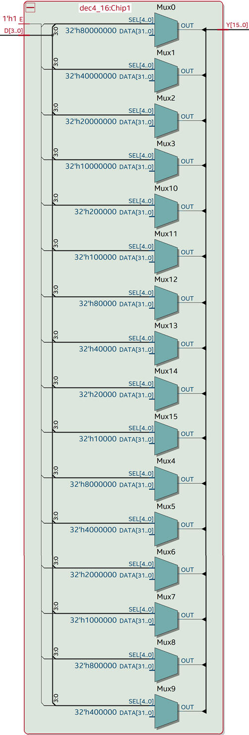 |
Fig. 4. RTL view of the Dec4_16 component elaborated using plan B. |
This is the VHDL translation ones_counter_4bit.vhd designed describing the architecture based on the MoD for implementing logic functions (Fig. 2).
 |
| Fig. 5. RTL view of 4-bit ones counter. |
Fig 6 shows the technology view. The circuit has four inputs, and thus only one logic element per output is required to complete the design.
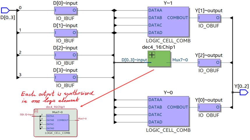 |
| Fig. 6. Technology view of 4-bit ones counter in three logic elements. |
4. Testing and validating the design (functional simulation)
In this example the simulation to verify the design has two phases: (1) Functional simulation, and (2) Gate-level simulation.
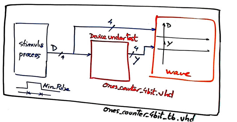
The testbench fixture to apply stimulus is represented in Fig. 7.
|
|
|
Fig. 7. Testbench construction to apply stimulus and visualise input and output ports. |
Let us perform the functional simulation:
Translate the sketch of an example timing diagram to a VHDL test bench (ones_counter_4bit_tb.vhd), meaning the skeleton of the testbench from Quartus Prime and then adding Min_Pulse constant to set the time resolution and the input stimulus process.
Run the VHDL simulation EDA tool ModelSim to obtain and discuss the timing diagram. This below is an example waveform:
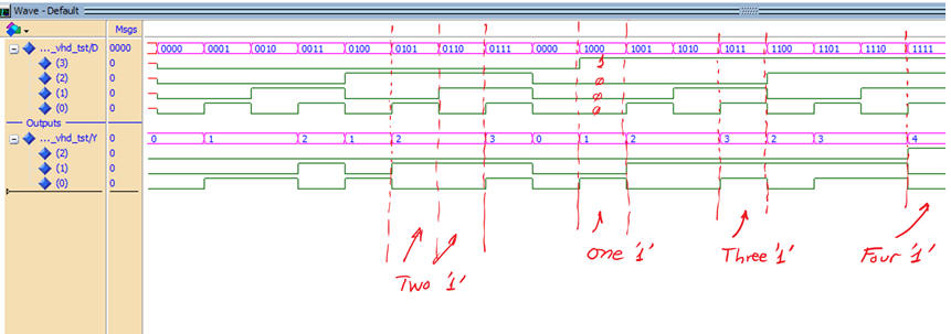 |
| Fig. 8. Waveforms for the 4-bit ones counter. |
5. Testing and validating the design (gate-level simulation)
Let us introduce the concept of gate-level simulations, where the detailed performance of the synthesised circuit can be examined and measured.
Select the correct option in Quartus Prime to allow generating SDO files, as shown in Fig. 9.
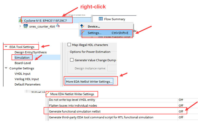 |
| Fig. 9. Generate SDO files associated to technology schematics. |
In Fig. 10 there is the list of generated files. Run gete-level simulations only with Cyclone IV and MAX II devices. MAX10 and other new FPGA do not generate SDO files.
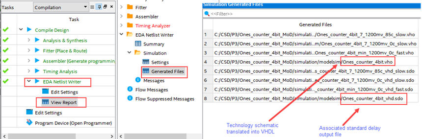 |
| Fig. 10. VHO and SDO files of interest for running gate-level simulations. |
Run ModelSim and setup a new gate-level project simulation. Use the same funcional simulation testbench file.
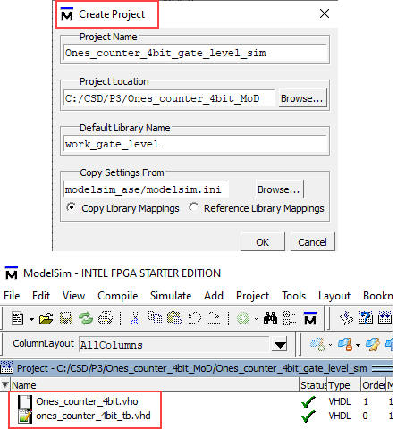 |
| Fig. 11. New gate level project including device under test and testbench files. |
Select to simulate the testbench and include the Ones_counter_4bit delay file.
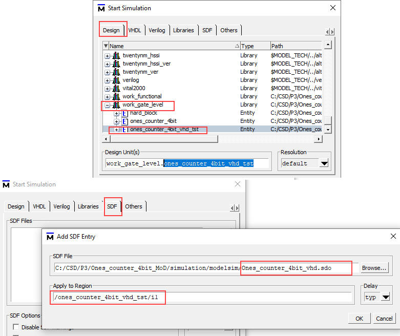 |
| Fig. 12. New gate level project including device under test and testbench files. |
Operate the logic analyser to observe:
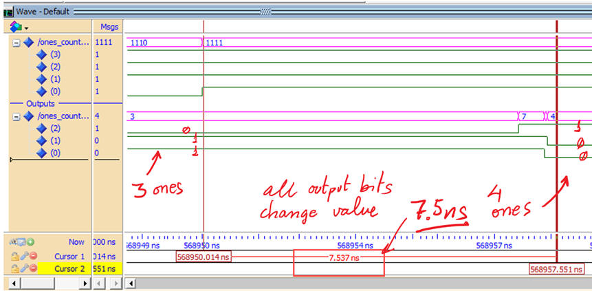
(1) Zoom all. Thus, the diagram must be the same as in Fig. 8.
(2) the behaviour of the output waveforms at a given transition (zooming in and in until you reach ns resolution. As you see here, it takes tP = 7.5 ns to obtain the correct count of ones. Note how every output has its own propagation time, and so we have to wait for the slowest signal to be set before having the correct result.
|
|
|
Fig. 13. Example of gate-level simulation where we can inspect the delay of the outputs at a given inputs transition. |
In order to compare the results from the simulator and the synthesiser, run the EDA tool timing analyser available in Quartus Prime to measure the worst-case scenario (longest propagation delay) and thus calculate the maximum speed of operation for a given target PFGA chip.
|
|
|
Fig. 14. Running timing analyser tool to measure the worst-case propagation delay. |
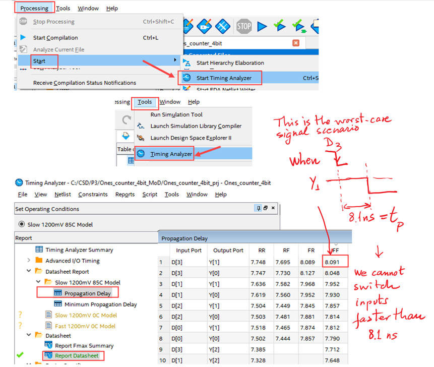
In this example the maximum processing speed is 123.5 MHz (about 125.5 millions of operations (counting the number of ones in the input vector) per second.
6. Report
Project report starting with the template sheets of paper, scanned figures, file listings, docx , pptx, or any other resources
7. Prototyping
Use training boards and perform laboratory measurements to verify how the circuit works.
| Home Term 26/27-Q1 Contact Products Electronic devices and companies Software Books Magazines Instruments DEE Library EETAC DEEL |

|
|
| Web activa des de 09/2001, @ F. J. Robert, Web editat amb Microsoft Expression Web 4. El contingut és un complement als materials d'estudi del curs Circuits i Sistemes Digitals disponibles al campus digital Atenea. Llicència:Reconeixement 4.0 Internacional de Creative Commons |