|
|
Bachelor's Degree in Telecommunications Systems and in Network Engineering |
|
|
|
(A) Wall clock (time) |
(B) Wall clock (time and date) |
Dedicated processor: datapath + control unit + CLK generator
| 1. Specifications | Planning | Developing | Test functional | Test gate-level | Prototype | Report |
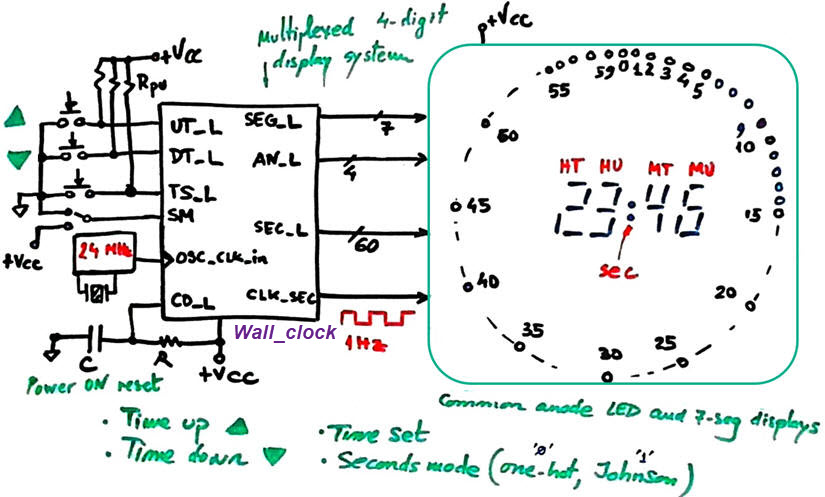
Design the typical wall clock for HH:MM and seconds represented in a 60 LED ring.
When clicking time set (TS_L) pushbutton the system enters the hours set mode and the display goes blinking. Clicking time up (TU_L) or time down (TD_L) pushbuttons allows fixing the hours from 00 to 23 counting fast at 10 Hz. Clicking again the minutes goes blinking and the same buttons are used for fixing minutes from 00 to 59. Clicking again you can set seconds LED in the same way. And a final TS_L click allows going back into normal clock operation. A switch (SM) seconds mode allows to select the 60 LED sphere in one-hot or in Johnson (shown in the photograph).
The 7-segment displays are multiplexed, so that only 11 wires are required for representing HH:MM. See an example of multiplexed display system MDS. On the other hand, we will drive 60 individual LED and also the seconds sign ":".
We can synthesise and test the circuit using Quartus Prime and ModelSim.
We can build and prototype this application using the MachXO starter kit or instead, one of our legacy FPGA boards.
 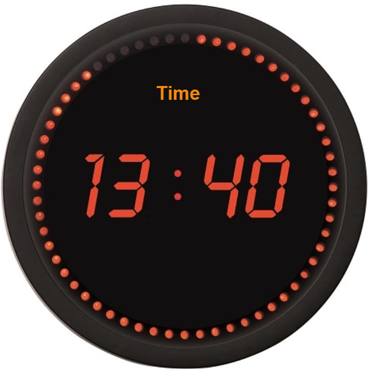 |
| Fig. 1. Symbol and example of commercial wall clock with seconds ring. |
This is another example of HH:MM:SS digital clock based on legacy sPLD GAL22V10 drawn in Proteus. We need several chained BCD counters to reach a counting modulo 24x60x60 = 86400.
| Specifications | 2. Planning | Developing | Test functional | Test gate-level | Prototype | Report |
Let us imagine a dedicated processor as shown in Fig. 2. The datapath will be in charge of counting real-time and also decoding hours, minutes and seconds. We will try to adapt and use all the required components from our library of products.
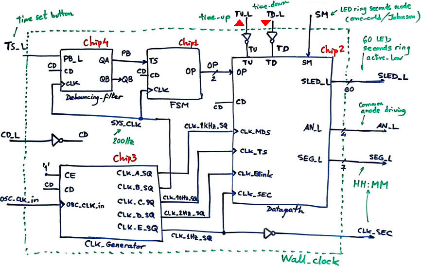 |
| Fig. 2. Planning the wall clock as a dedicated processor. |
We will use the FSM recipe for implementing the control unit Chip1 accordingly to the Fig. 3 state diagram. Four modes of operation will be selected clicking the time set (TS) push-button.
To generate a synchronous single pulse per click we can use the output QA of the Chip4 Debouncing circuit.
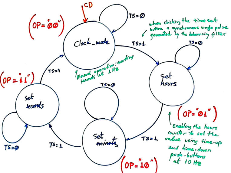 |
| Fig. 3. FSM state diagram. |
The datapath will require several components for counting, multiplexing and decoding.
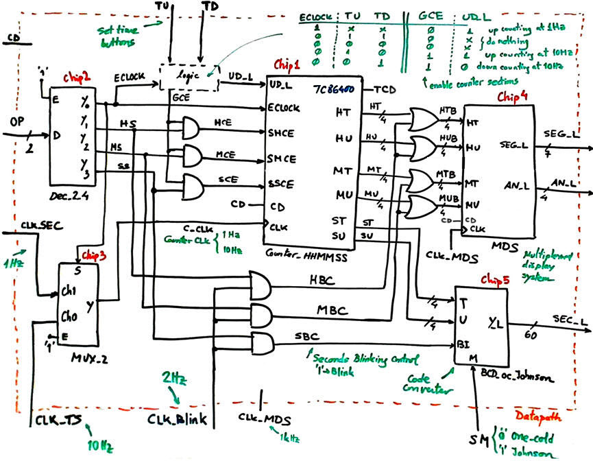 |
| Fig. 4. Datapath structure based on a Counter_HHMMSS, a one day modulo 84600 counter that will allow individual enabling of hours, minutes and seconds. The multiplexed 7-segment display system and the seconds LED decoder code converter is also included. |
The key operational component for the real-time clock is the counter modulo 84600 consisting of three sections: hours, minutes and seconds. The general enable clock (ECLOCK) chains the three sections (24x60x60) to count using the 1 Hz time-base. Each section includes a particular count enable (SHCE, SMCE and SSCE) for allowing setting the time at higher speed (10 Hz) using TU and TD push-buttons.
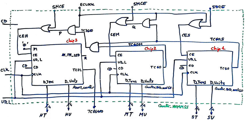 |
| Fig. 5. One day real-time counter based on chaining hours, minutes and seconds components. |
Chip1 and Chip2 come from the highlighted Timer_MMSS in P8. Chip3 Hours_counter is highlighted in P7.
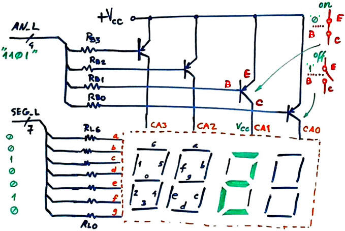
Chip4 in Fig. 4 will drive up to four 7-segment displays (HH:MM) using a time multiplexing technique to reduce drastically the number of pins required (11 pins instead of 28).
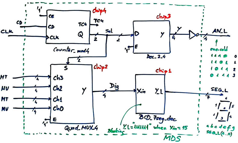  |
| Fig. 6. The MDS adapted from its tutorial. |
Chip5 in the datapath is a code converter from BCD modulo 60 to one-cold or Johnson, depending on the control input mode (M). Blanking control is achieved switching off all sixty LED. We can try to synthesise this circuit using plan B, which is basically translating its true table into VHDL. Alternatively, we can try to invent it using smaller components of the same kind applying plan C2.
Another interesting way to solve the seconds counter (Chip1 in Fig. 4) to drive sixty LED while avoiding this code translator is to plan it directly as Counter_oc_Johnson_60bit (plan Y) adapting for example the tutorial Counter_BCD_1digit.
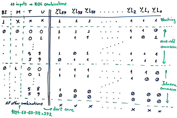 |
| Fig. 7. The code converter truth table to obtain from BCD units and tens to final active-low one-cold or Johnson codes for driving the sixty LED ring to display the seconds count. |
As shown in Fig. 8, we will implement using plan C2 the CLK_Generator Chip3 in Fig. 2 as explained in L8.1. Several square wave are required in this application: 200 Hz to run the system and sample the time set push-button; 1 kHz for the multiplexed display system; 10 Hz for speeding the time set when clicking time-up and time -down push-buttons; 2 Hz for blinking the corresponding counter section when setting time; and 1 Hz for normal operation.
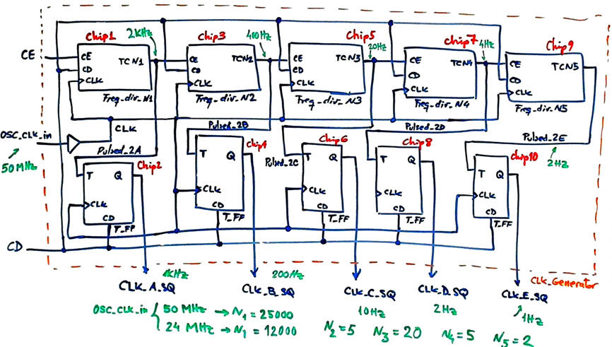 |
| Fig. 8. The proposed CLK_Generator. |
This is the project location:
C:\CSD\P8\Wall_clock\(files)
| Specifications | Planning | 3. Developing | Test functional | Test gate-level | Prototype | Report |
| Specifications | Planning | Developing | 4. Test functional | Test gate-level | Prototype | Report |
| Specifications | Planning | Developing | Test functional | 5. Test gate-level | Prototype | Report |
| Specifications | Planning | Developing | Test functional | Test gate-level | 6. Prototype | Report |
| Specifications | Planning | Developing | Test functional | Test gate-level | Prototype | 7. Report |
Follow this rubric for writing reports.
|
|
(A) Wall clock (time) |
(B) Wall clock (time and date) |
| 1. Specifications | Planning | Developing | Test functional | Test gate-level | Prototype | Report |
This is another similar design including time and date. It also includes room temperature monitoring. Instead of designing all the modules, we better try to interface a real-time clock calendar type Maxim's DS1307.
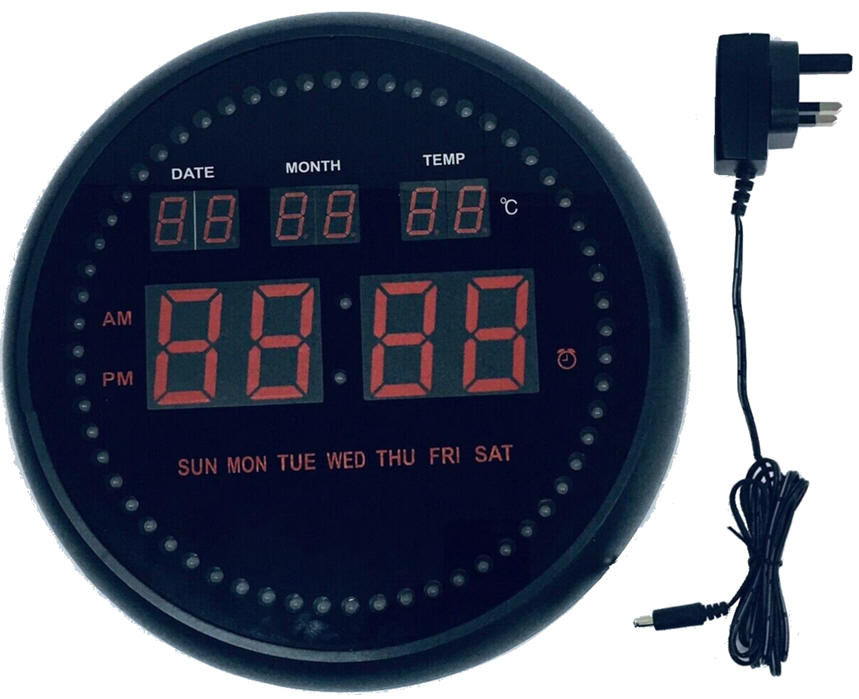 |
| Fig. 1. Initial picture from where to start imagining the circuit's symbol. |
| Specifications | 2. Planning | Developing | Test functional | Test gate-level | Prototype | Report |
| Specifications | Planning | 3. Developing | Test functional | Test gate-level | Prototype | Report |
| Specifications | Planning | Developing | 4. Test functional | Test gate-level | Prototype | Report |
| Specifications | Planning | Developing | Test functional | 5. Test gate-level | Prototype | Report |
| Specifications | Planning | Developing | Test functional | Test gate-level | 6. Prototype | Report |
| Specifications | Planning | Developing | Test functional | Test gate-level | Prototype | 7. Report |
Follow this rubric for writing reports.
| Home Term 26/27-Q1 Contact Products Electronic devices and companies Software Books Magazines Instruments DEE Library EETAC DEEL |

|
|
| Web activa des de 09/2001, @ F. J. Robert, Web editat amb Microsoft Expression Web 4. El contingut és un complement als materials d'estudi del curs Circuits i Sistemes Digitals disponibles al campus digital Atenea. Llicència:Reconeixement 4.0 Internacional de Creative Commons |