

|
Bachelor's Degree in Telecommunications Systems and in Network Engineering |

|
|
|
||
|
|
BCD counter modulo 60 (seconds or minutes counter) |
|
|
|
||
| 1. Specifications | Planning | Developing | Test functional | Test gate-level | Report | Prototype |
The objective is to design a minutes or seconds counter suitable for real-time clock devices. The counter operates cyclically in binary-coded decimal (BCD) from 00 to 59, justifying the designation Counter_BCD_mod60.
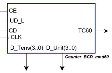
The design process is structured into several progressive stages. First, the basic up-counter circuit is established, as illustrated by the symbol in Fig. 1. Next, reversibility is implemented to allow for both up and down counting. Finally, as one of the components to be used for the Timer_MMSS (version C) project, parallel inputs are integrated to facilitate the pre-loading of initial counts.
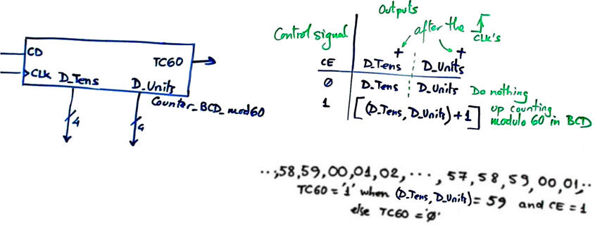 |
Fig 1. Initial symbol and function table for the proposed 2-digit BCD counter up to modulo 60. |
To complete the initial specification, you can draw an example of timing diagram.
 |
|
Fig. 2. Timing diagram example. |
| Specifications | 2. Planning | Developing | Test functional | Test gate-level | Report | Prototype |
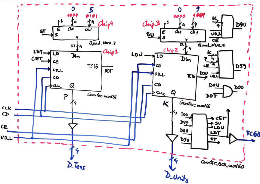
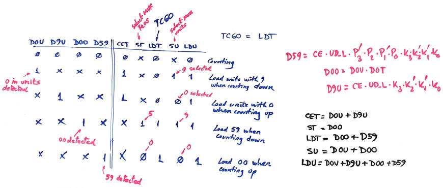
The implementation will proceed according to Plan C2. Developing a BCD modulo-60 counter requires cascading Counter_mod16 components using the truncation techniques detailed in Lecture L7.3. By adapting the BCD modulo-24 counter from project P7, the final design will support bidirectional (up/down) counting functionality.
 |
|
| Fig 3. Proposed internal architecture for Counter_BCD_mod60. |
Project location:
C:\CSD\P7\Counter_BCD_mod60\(files)
| Specifications | Planning | 3. Developing | Test functional | Test gate-level | Report | Prototype |
Example file translation of schematics above in Fig. 3: Counter_BCD_mod60.vhd, Quad_MUX_2.vhd, and copy the Counter_mod16.vhd from its plan Y tutorial Counter_mod16.
You can use Quartus Prime and any convenient Intel FPGA, for instance a Cyclone IV, as target chip to synthesise this project.
|
|
|
Fig. 4. RTL |
|
|
|
Fig. 5. Technology view and resources used in the design. |
| Specifications | Planning | Developing | 4. Test functional | Test gate-level | Report | Prototype |
The testbench fixture.
|
|
|
Fig. 6. Testbench fixture for connecting stimulus process to the unit under test. |
|
|
|
Fig. 7. ModelSim wave diagram. |
| Specifications | Planning | Developing | Test functional | 5. Test gate-level | Report | Prototype |
In this section we can repeat measurements simulating propagation delays
|
|
|
Fig. 8. ModelSim wave diagram zooming a transition for measururing the parameter propagation time from CLK to output tCO. |
| Specifications | Planning | Developing | Test functional | Test gate-level | 6. Report | Prototype |
Follow this rubric for writing reports.
| Specifications | Planning | Developing | Test functional | Test gate-level | Report | 7. Prototype |
We built and use this module in several training and demonstration designs:
A) Timer_MMSS, P8 highlighted project as one of the components of the Counter_BCD_MMSS.
B) Prototype in a legacy NIOS board. Target chip: APEX EP20K200EFC484-2X.
C) Prototype in a legacy UP2 board. Target chips: EPM7128SLC84-7 and FLEX EPF10K70RC240-4.
| Home Term 26/27-Q1 Contact Products Electronic devices and companies Software Books Magazines Instruments DEE Library EETAC DEEL |

|

|
| Web activa des de 09/2001, @ F. J. Robert, Web editat amb Microsoft Expression Web 4. El contingut és un complement als materials d'estudi del curs Circuits i Sistemes Digitals disponibles al campus digital Atenea. Llicència:Reconeixement 4.0 Internacional de Creative Commons |